Материал: MJE18002
MOTOROLA
SEMICONDUCTOR TECHNICAL DATA
Order this document by MJE18002/D
Designer's Data Sheet
SWITCHMODE
NPN Bipolar Power Transistor
For Switching Power Supply Applications
The MJE/MJF18002 have an applications specific state±of±the±art die designed for use in 220 V line operated Switchmode Power supplies and electronic light ballasts. These high voltage/high speed transistors offer the following:
•Improved Efficiency Due to Low Base Drive Requirements:
ÐHigh and Flat DC Current Gain h FE
ÐFast Switching
ÐNo Coil Required in Base Circuit for Turn±Off (No Current Tail)
•Tight Parametric Distributions are Consistent Lot±to±Lot
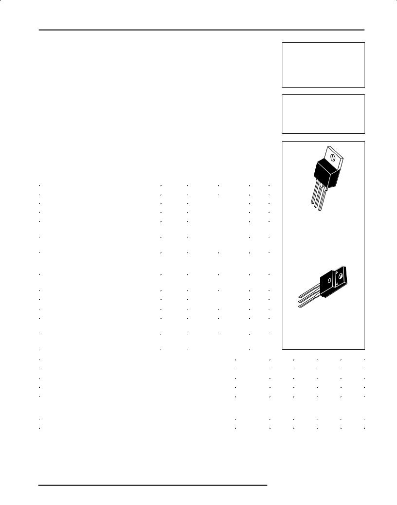
•Two Package Choices: Standard TO±220 or Isolated TO±220
•MJF18002, Case 221D, is UL Recognized at 3500 VRMS: File #E69369
MAXIMUM RATINGS
Rating |
|
Symbol |
MJE18002 |
MJF18002 |
Unit |
|
|
|
|
|
|
|
|
Collector±Emitter Sustaining Voltage |
VCEO |
|
450 |
Vdc |
||
Collector±Emitter Breakdown Voltage |
VCES |
|
1000 |
Vdc |
||
Emitter±Base Voltage |
|
VEBO |
|
9.0 |
Vdc |
|
Collector Current Ð Continuous |
IC |
|
2.0 |
Adc |
||
Ð Peak(1) |
|
ICM |
|
5.0 |
|
|
Base Current Ð Continuous |
|
IB |
|
1.0 |
Adc |
|
Ð Peak(1) |
|
IBM |
|
2.0 |
|
|
RMS Isolated Voltage(2) |
Test No. 1 Per Fig. 1 |
VISOL |
Ð |
|
4500 |
V |
(for 1 sec, R.H. < 30%, |
Test No. 2 Per Fig. 2 |
|
Ð |
|
3500 |
|
TC = 25°C) |
Test No. 3 Per Fig. 3 |
|
Ð |
|
1500 |
|
Total Device Dissipation |
(TC = 25°C) |
PD |
50 |
|
25 |
Watts |
Derate above 25°C |
|
|
0.4 |
0.2 |
W/°C |
|
|
|
|
|
|
|
|
Operating and Storage Temperature |
TJ, Tstg |
|
± 65 to 150 |
°C |
||
THERMAL CHARACTERISTICS |
|
|
|
|
|
|
Rating |
Symbol |
MJE18002 |
MJF18002 |
Unit |
|
|
|
|
|
Thermal Resistance Ð Junction to Case |
RqJC |
2.5 |
5.0 |
°C/W |
Ð Junction to Ambient |
RqJA |
62.5 |
62.5 |
|
Maximum Lead Temperature for Soldering |
TL |
260 |
°C |
|
Purposes: 1/8″ from Case for 5 Seconds |
|
|
|
|
ELECTRICAL CHARACTERISTICS (TC = 25°C unless otherwise noted)
MJE18002* MJF18002*
*Motorola Preferred Device
POWER TRANSISTOR
2.0 AMPERES
1000 VOLTS
25 and 50 WATTS
CASE 221A±06
TO±220AB
MJE18002
CASE 221D±02
ISOLATED TO±220 TYPE
UL RECOGNIZED
MJF18002
Characteristic |
|
Symbol |
Min |
Typ |
Max |
|
Unit |
|
|
|
|
|
|
|
|
OFF CHARACTERISTICS |
|
|
|
|
|
|
|
|
|
|
|
|
|
|
|
Collector±Emitter Sustaining Voltage (IC = 100 mA, L = 25 mH) |
|
VCEO(sus) |
450 |
Ð |
Ð |
|
Vdc |
Collector Cutoff Current (VCE = Rated VCEO, IB = 0) |
|
ICEO |
Ð |
Ð |
100 |
|
mAdc |
Collector Cutoff Current (VCE = Rated VCES, VEB = 0) |
TC = 125°C |
ICES |
Ð |
Ð |
100 |
|
mAdc |
Collector Cutoff Current (VCE = 800 V, VEB = 0) |
TC = 125°C |
|
Ð |
Ð |
500 |
|
|
|
|
|
Ð |
Ð |
100 |
|
|
|
|
|
|
|
|
|
|
Emitter Cutoff Current (VEB = 9.0 Vdc, IC = 0) |
|
IEBO |
Ð |
Ð |
100 |
|
mAdc |
(1) Pulse Test: Pulse Width = 5.0 ms, Duty Cycle ≤ 10%. |
|
|
|
|
|
(continued) |
|
(2) Proper strike and creepage distance must be provided. |
|
|
|
|
|
|
|
Designer's Data for ªWorst Caseº Conditions Ð The Designer 's Data Sheet permits the design of most circuits entirely from the information presented. SOA Limit curves Ð representing boundaries on device characteristics Ð are given to facilitate ªworst caseº design.
Preferred devices are Motorola recommended choices for future use and best overall value.
Designer's and SWITCHMODE are trademarks of Motorola, Inc.
REV 1
Motorola, Inc. 1995

MJE18002 MJF18002
ELECTRICAL CHARACTERISTICS Ð continued (TC = 25°C unless otherwise noted)
|
|
|
|
Characteristic |
|
|
|
Symbol |
|
Min |
Typ |
Max |
Unit |
|
|
|
|
|
|
|
|
|
|
|
|
|
|
|
|
ON CHARACTERISTICS |
|
|
|
|
|
|
|
|
|
|
|
|
|
|
|
|
|
|
|
|
|
|
|
|
|
|
|||
Base±Emitter Saturation Voltage |
(IC = 0.4 Adc, IB = 40 mAdc) |
|
VBE(sat) |
|
Ð |
0.825 |
1.1 |
Vdc |
||||||
Base±Emitter Saturation Voltage |
(IC = 1.0 Adc, IB = 0.2 Adc) |
|
|
|
Ð |
0.92 |
1.25 |
|
||||||
Collector±Emitter Saturation Voltage |
|
|
|
VCE(sat) |
|
|
|
|
Vdc |
|||||
(IC = 0.4 Adc, IB = 40 mAdc) |
|
|
@ TC = 125°C |
|
|
Ð |
0.2 |
0.5 |
|
|||||
(IC = 1.0 Adc, IB = 0.2 Adc) |
|
|
|
|
Ð |
0.2 |
0.5 |
|
||||||
|
|
@ TC = 125°C |
|
|
Ð |
0.25 |
0.5 |
|
||||||
|
|
|
|
|
|
|
|
|
Ð |
0.3 |
0.6 |
|
||
|
|
|
|
|
|
|
|
|
|
|
|
|||
DC Current Gain (IC = 0.2 Adc, VCE = 5.0 Vdc) |
|
@ TC = 125°C |
hFE |
|
14 |
Ð |
34 |
Ð |
||||||
|
|
|
|
|
|
|
|
|
Ð |
27 |
Ð |
|
||
DC Current Gain (IC = 0.4 Adc, VCE = 1.0 Vdc) |
|
@ TC = 125°C |
|
|
11 |
17 |
Ð |
|
||||||
|
|
|
|
|
|
|
|
|
11 |
20 |
Ð |
|
||
DC Current Gain (IC = 1.0 Adc, VCE = 1.0 Vdc) |
|
@ TC = 125°C |
|
|
6.0 |
8.0 |
Ð |
|
||||||
|
|
|
|
|
|
|
|
|
5.0 |
8.0 |
Ð |
|
||
DC Current Gain (IC = 10 mAdc, VCE = 5.0 Vdc) |
|
|
|
|
|
10 |
20 |
Ð |
|
|||||
DYNAMIC CHARACTERISTICS |
|
|
|
|
|
|
|
|
|
|
||||
|
|
|
|
|
|
|
|
|
|
|||||
Current Gain Bandwidth (IC = 0.2 Adc, VCE = 10 Vdc, f = 1.0 MHz) |
fT |
|
Ð |
13 |
Ð |
MHz |
||||||||
Output Capacitance (VCB = 10 Vdc, IE = 0, f = 1.0 MHz) |
|
|
Cob |
|
Ð |
35 |
60 |
pF |
||||||
Input Capacitance (VEB = 8.0 V) |
|
|
|
|
Cib |
|
Ð |
400 |
600 |
pF |
||||
Dynamic Saturation: |
|
|
IC = 0.4 A |
1.0 μs |
|
= 125°C |
VCE(dsat) |
|
Ð |
3.5 |
Ð |
Vdc |
||
|
|
|
|
@ T |
|
|
Ð |
8.0 |
Ð |
|
||||
determined 1.0 μs and |
|
IB1 = 40 mA |
|
C |
|
|
|
|
|
|
|
|||
|
|
|
|
|
|
Ð |
1.5 |
Ð |
|
|||||
3.0 μs after rising I |
|
|
VCC = 300 V |
3.0 μs |
|
|
|
|
|
|||||
B1 |
|
|
|
|
|
@ TC = 125°C |
|
|
Ð |
3.8 |
Ð |
|
||
reach 0.9 final IB1 |
|
|
|
|
|
|
|
|
||||||
|
|
|
|
|
|
|
|
|
Ð |
8.0 |
Ð |
|
||
(see Figure 18) |
|
|
IC = 1.0 A |
1.0 μs |
|
= 125°C |
|
|
|
|||||
|
|
|
|
@ TC |
|
|
Ð |
14 |
Ð |
|
||||
|
|
|
|
|
|
|
|
|||||||
|
|
|
|
IB1 = 0.2 A |
|
|
|
|
|
|
|
|
|
|
|
|
|
|
|
|
|
|
|
Ð |
2.0 |
Ð |
|
||
|
|
|
|
VCC = 300 V |
3.0 μs |
|
|
|
|
|
||||
|
|
|
|
@ TC |
= 125°C |
|
|
Ð |
7.0 |
Ð |
|
|||
|
|
|
|
|
|
|
|
|
|
|||||
SWITCHING CHARACTERISTICS: Resistive Load (D.C. ≤ 10%, Pulse Width = 20 μs) |
|
|
|
|
||||||||||
|
|
|
|
|
|
|
|
|
|
|
||||
Turn±On Time |
|
IC = 0.4 Adc |
|
@ TC = 125°C |
ton |
|
Ð |
200 |
300 |
ns |
||||
|
|
IB1 = 40 mAdc |
|
|
|
Ð |
130 |
Ð |
|
|||||
|
|
IB2 = 0.2 Adc |
|
|
|
|
|
|
|
|
|
|||
Turn±Off Time |
|
|
|
|
toff |
|
Ð |
1.2 |
2.5 |
μs |
||||
|
VCC = 300 V |
|
@ TC = 125°C |
|
||||||||||
|
|
|
|
|
Ð |
1.5 |
Ð |
|
||||||
|
|
|
|
|
|
|
|
|
|
|||||
Turn±On Time |
|
IC = 1.0 Adc |
|
@ TC = 125°C |
ton |
|
Ð |
85 |
150 |
ns |
||||
|
|
IB1 = 0.2 Adc |
|
|
|
Ð |
95 |
Ð |
|
|||||
|
|
IB2 = 0.5 Adc |
|
|
|
|
|
|
|
|
|
|||
Turn±Off Time |
|
|
|
|
toff |
|
Ð |
1.7 |
2.5 |
μs |
||||
|
|
VCC = 300 V |
|
@ TC = 125°C |
|
|
Ð |
2.1 |
Ð |
|
||||
SWITCHING CHARACTERISTICS: Inductive Load (Vclamp = 300 V, VCC = 15 V, L = 200 μH) |
|
|
|
|
||||||||||
Fall Time |
|
|
IC = 0.4 Adc, IB1 = 40 mAdc, |
@ TC = 125°C |
tfi |
|
Ð |
125 |
200 |
ns |
||||
|
|
|
|
|
IB2 = 0.2 Adc |
|
|
|
Ð |
120 |
Ð |
|
||
Storage Time |
|
|
|
|
|
|
@ TC = 125°C |
tsi |
|
Ð |
0.7 |
1.25 |
μs |
|
|
|
|
|
|
|
|
|
|
Ð |
0.8 |
Ð |
|
||
Crossover Time |
|
|
|
|
|
|
@ TC = 125°C |
tc |
|
Ð |
110 |
200 |
ns |
|
|
|
|
|
|
|
|
|
|
Ð |
110 |
Ð |
|
||
Fall Time |
|
|
IC = 1.0 Adc, IB1 = 0.2 Adc, |
@ TC = 125°C |
tfi |
|
Ð |
110 |
175 |
ns |
||||
|
|
|
|
|
IB2 = 0.5 Adc |
|
|
|
Ð |
120 |
Ð |
|
||
Storage Time |
|
|
|
|
|
|
@ TC = 125°C |
tsi |
|
Ð |
1.7 |
2.75 |
μs |
|
|
|
|
|
|
|
|
|
|
Ð |
2.25 |
Ð |
|
||
Crossover Time |
|
|
|
|
|
|
@ TC = 125°C |
tc |
|
Ð |
200 |
300 |
ns |
|
|
|
|
|
|
|
|
|
|
Ð |
250 |
Ð |
|
||
Fall Time |
|
|
IC = 0.4 Adc, IB1 = 50 mAdc, |
@ TC = 125°C |
tfi |
|
Ð |
140 |
200 |
ns |
||||
|
|
|
|
|
IB2 = 50 mAdc |
|
|
|
Ð |
185 |
Ð |
|
||
Storage Time |
|
|
|
|
|
|
@ TC = 125°C |
tsi |
|
Ð |
2.2 |
3.0 |
μs |
|
|
|
|
|
|
|
|
|
|
Ð |
2.5 |
Ð |
|
||
Crossover Time |
|
|
|
|
|
|
@ TC = 125°C |
tc |
|
Ð |
140 |
250 |
ns |
|
|
|
|
|
|
|
|
|
|
Ð |
220 |
Ð |
|
||
2 |
Motorola Bipolar Power Transistor Device Data |
MJE18002 MJF18002
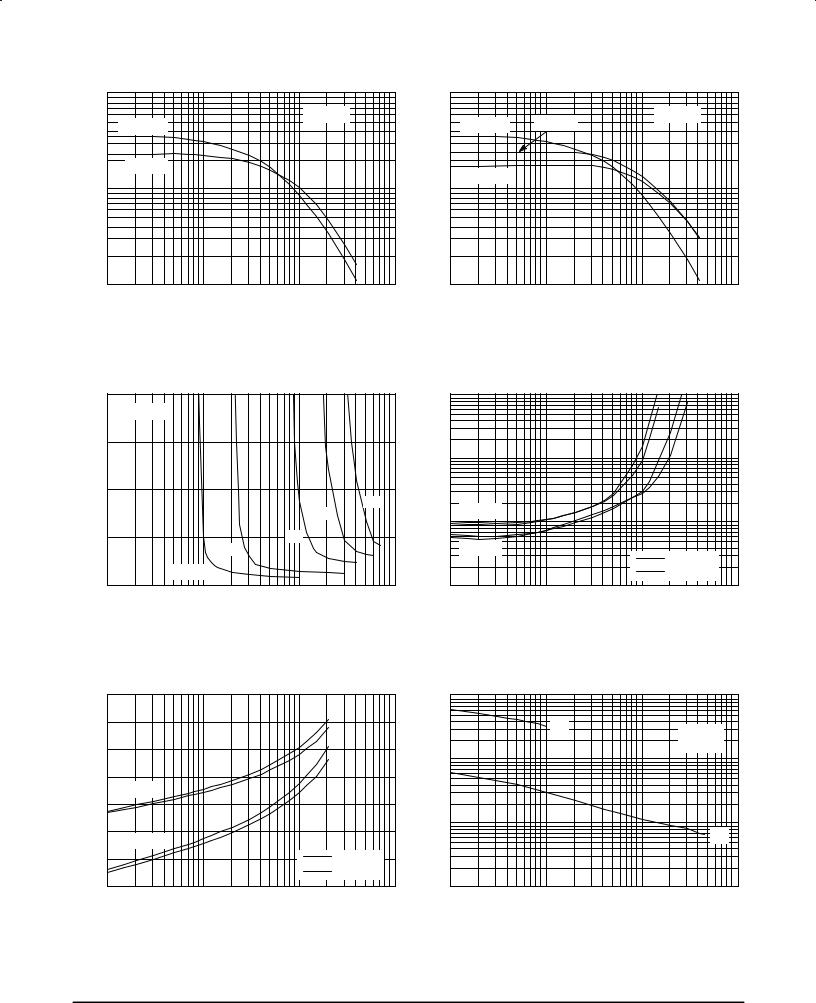
TYPICAL STATIC CHARACTERISTICS
|
100 |
|
|
|
|
100 |
|
|
|
|
|
TJ = 125°C |
VCE = 1 V |
|
|
TJ = 125°C |
TJ = 25°C |
VCE = 5 V |
|
GAIN |
|
|
|
GAIN |
|
|
|||
|
|
|
|
|
|
|
|
||
, DC CURRENT |
|
TJ = 25°C |
|
|
, DC CURRENT |
TJ = ± 20°C |
|
|
|
10 |
|
|
|
|
|
|
|||
|
|
|
10 |
|
|
|
|||
|
|
|
|
|
|
|
|
||
FE |
|
|
|
|
FE |
|
|
|
|
h |
|
|
|
|
h |
|
|
|
|
|
1 |
|
|
|
|
1 |
|
|
|
|
0.01 |
0.10 |
1.00 |
10.00 |
|
0.01 |
0.10 |
1.00 |
10.00 |
|
|
IC, COLLECTOR CURRENT (AMPS) |
|
|
|
IC, COLLECTOR CURRENT (AMPS) |
|
||
Figure 1. DC Current Gain @ 1 Volt |
Figure 2. DC Current Gain @ 5 Volts |
VCE, VOLTAGE (VOLTS)
2 |
|
|
|
|
10.00 |
|
|
|
|
|
TJ = 25°C |
|
|
|
|
|
|
|
|
|
|
|
|
(VOLTS) |
|
1.00 |
|
|
|
1 |
|
1.5 A |
|
VOLTAGE, |
|
|
IC/IB = 10 |
|
|
|
|
|
|
|
|
|
|
|
|
|
|
|
2 A |
|
|
|
|
|
|
|
|
|
|
CE |
0.10 |
|
|
|
|
|
|
|
|
|
|
|
|
||
|
|
1 A |
|
V |
|
|
|
|
|
|
|
|
|
|
|
IC/IB = 5 |
|
|
|
|
|
0.4 A |
|
|
|
|
|
TJ = 25°C |
|
|
|
|
|
|
|
|
|
|
|
0 |
IC = 0.2 A |
|
|
|
|
0.01 |
|
|
TJ = 125°C |
0.001 |
0.010 |
0.100 |
1.000 |
|
|
0.01 |
0.10 |
1.00 |
10.00 |
|
IB, BASE CURRENT (mA) |
|
|
|
|
IC, COLLECTOR CURRENT (AMPS) |
|
||
Figure 3. Collector Saturation Region |
Figure 4. Collector±Emitter Saturation Voltage |
VBE, VOLTAGE (VOLTS)
1.1 |
|
|
|
|
1000 |
|
|
|
1.0 |
|
|
|
|
|
|
Cib |
TJ = 25°C |
|
|
|
|
|
|
|
||
0.9 |
|
|
|
(pF) |
100 |
|
|
f = 1 MHz |
|
|
|
|
|
|
|
||
|
|
|
|
CAPACITANCE |
|
|
|
|
0.8 |
|
|
|
|
|
|
|
|
|
|
|
|
|
|
|
|
|
TJ = 25°C |
|
|
|
|
|
|
|
|
0.7 |
|
|
|
|
|
|
|
|
0.6 |
|
|
|
C, |
10 |
|
|
|
|
|
|
|
|
|
Cob |
||
TJ = 125°C |
|
|
|
|
|
|
|
|
0.5 |
|
|
IC/IB = 10 |
|
|
|
|
|
0.4 |
|
|
IC/IB = 5 |
|
1 |
|
|
|
0.01 |
0.10 |
1.00 |
10.00 |
|
1 |
10 |
100 |
1000 |
|
IC, COLLECTOR CURRENT (AMPS) |
|
|
|
VCE, COLLECTOR±EMITTER (VOLTS) |
|
||
Figure 5. Base±Emitter Saturation Region |
Figure 6. Capacitance |
Motorola Bipolar Power Transistor Device Data |
3 |
MJE18002 MJF18002
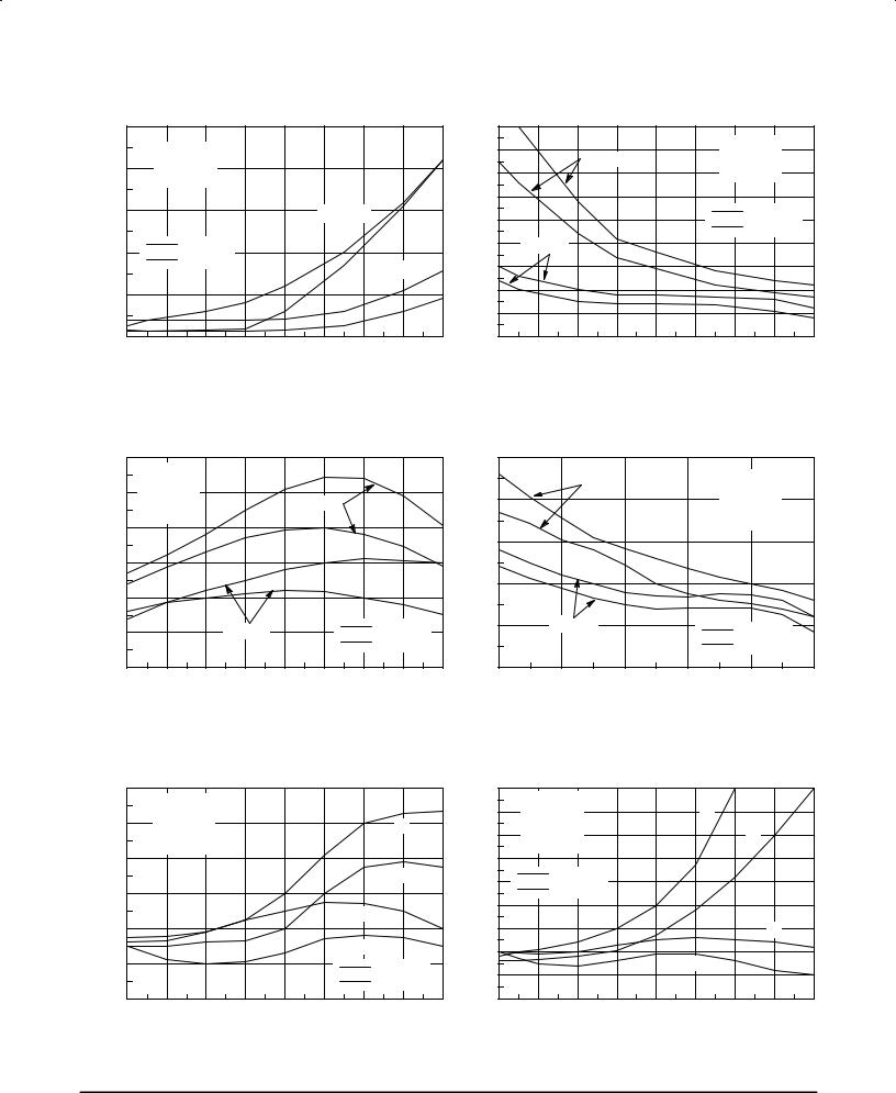
TYPICAL SWITCHING CHARACTERISTICS (IB2 = IC/2 for all switching)
|
2500 |
|
|
|
|
|
|
|
|
|
|
IB(off) = IC/2 |
|
|
|
|
|
|
|
|
2000 |
VCC = 300 V |
|
|
|
|
|
|
|
|
|
PW = 20 μs |
|
|
|
|
|
|
|
(ns) |
1500 |
|
|
|
|
TJ = 125°C |
|
(ns) |
|
|
|
|
|
|
|
||||
t, TIME |
1000 |
|
IC/IB = 5 |
|
|
|
|
|
t, TIME |
|
|
|
IC/IB = 10 |
|
|
|
|
TJ = 25°C |
|
|
|
|
|
|
|
|
|
|
|
|
500 |
|
|
|
|
|
|
|
|
|
0 |
|
|
|
|
|
|
|
|
|
0.4 |
0.6 |
0.8 |
1.0 |
1.2 |
1.4 |
1.6 |
1.8 |
2.0 |
IC, COLLECTOR CURRENT (AMPS)
4500 |
|
|
|
|
|
|
|
|
4000 |
|
|
IC/IB = 5 |
|
|
IB(off) = IC/2 |
|
|
3500 |
|
|
|
|
VCC = 300 V |
|
||
|
|
|
|
|
PW = 20 |
μ |
|
|
|
|
|
|
|
|
s |
|
|
3000 |
|
|
|
|
|
|
|
|
2500 |
|
|
|
|
|
TJ = 25°C |
|
|
2000 |
|
|
|
|
|
TJ = 125°C |
|
|
IC/IB = 10 |
|
|
|
|
|
|
|
|
|
|
|
|
|
|
|
|
|
1500 |
|
|
|
|
|
|
|
|
1000 |
|
|
|
|
|
|
|
|
500 |
|
|
|
|
|
|
|
|
0 |
|
|
|
|
|
|
|
|
0.4 |
0.6 |
0.8 |
1.0 |
1.2 |
1.4 |
1.6 |
1.8 |
2.0 |
|
|
IC, COLLECTOR CURRENT (AMPS) |
|
|
||||
Figure 7. Resistive Switching, ton |
Figure 8. Resistive Switching, toff |
|
3000 |
|
|
|
|
|
|
|
|
|
|
IB(off) = IC/2 |
|
|
|
|
|
|
|
|
2500 |
VCC = 15 V |
|
|
|
IC/IB = 5 |
|
|
|
|
|
VZ = 300 V |
|
|
|
|
|
|
|
|
2000 |
LC = 200 μH |
|
|
|
|
|
|
|
|
|
|
|
|
|
|
|
|
|
(ns) |
|
|
|
|
|
|
|
|
|
t, TIME |
1500 |
|
|
|
|
|
|
|
|
1000 |
|
|
|
|
|
|
|
|
|
|
|
|
|
|
|
|
|
|
|
|
500 |
|
I |
/I = 10 |
|
|
|
TJ = 25°C |
|
|
|
|
|
C B |
|
|
|
TJ = 125°C |
|
|
|
|
|
|
|
|
|
|
|
|
0 |
|
|
|
|
|
|
|
|
|
0.4 |
0.6 |
0.8 |
1.0 |
1.2 |
1.4 |
1.6 |
1.8 |
2.0 |
|
|
|
IC, COLLECTOR CURRENT (AMPS) |
|
|
||||
|
2500 |
|
|
|
|
|
|
|
|
IC = 1 A |
|
IB(off) = IC/2 |
|
|
2000 |
|
|
|
VCC = 15 V |
|
(ns) |
|
|
|
|
VZ = 300 V |
|
|
|
|
|
LC = 200 μH |
|
|
TIME |
|
|
|
|
|
|
1500 |
|
|
|
|
|
|
|
|
|
|
|
|
|
, STORAGE |
1000 |
|
|
|
|
|
|
|
|
|
|
|
|
si |
|
|
|
|
|
|
t |
500 |
IC = 0.4 A |
|
|
|
|
|
|
TJ = 25°C |
|
|||
|
|
|
|
|
TJ = 125°C |
|
|
0 |
|
|
|
|
|
|
5 |
7 |
9 |
11 |
13 |
15 |
|
|
|
hFE, FORCED GAIN |
|
|
|
Figure 9. Inductive Storage Time, tsi |
Figure 10. Inductive Storage Time |
|
600 |
|
|
|
|
|
|
|
|
|
|
IB(off) = IC/2 |
|
|
|
|
|
|
|
|
500 |
VCC = 15 V |
|
|
|
|
tc |
|
|
|
|
VZ = 300 V |
|
|
|
|
|
||
|
400 |
LC = 200 μH |
|
|
|
|
|
|
|
|
|
|
|
|
|
|
|
|
|
(ns) |
|
|
|
|
|
|
|
tfi |
|
t, TIME |
300 |
|
|
|
|
|
|
|
|
|
|
|
|
|
|
tc |
|
|
|
|
200 |
|
|
|
|
|
|
|
|
|
|
|
|
|
|
|
|
|
|
|
100 |
|
|
|
|
|
tfi |
|
|
|
|
|
|
|
|
|
TJ = 25°C |
|
|
|
|
|
|
|
|
|
|
|
|
|
0 |
|
|
|
|
|
|
TJ = 125°C |
|
|
|
|
|
|
|
|
|
|
|
|
0.4 |
0.6 |
0.8 |
1.0 |
1.2 |
1.4 |
1.6 |
1.8 |
2.0 |
|
|
|
IC, COLLECTOR CURRENT (AMPS) |
|
|
||||
|
450 |
IB(off) = IC/2 |
|
|
|
|
|
|
|
|
400 |
|
|
|
tc |
|
|
||
|
VCC = 15 V |
|
|
|
|
|
|||
|
350 |
VZ = 300 V |
|
|
|
|
tfi |
|
|
|
300 |
LC = 200 μH |
|
|
|
|
|
|
|
|
|
|
|
|
|
|
|
|
|
(ns) |
250 |
|
TJ = 25°C |
|
|
|
|
|
|
TIME |
200 |
|
TJ = 125°C |
|
|
|
|
|
|
t, |
|
|
|
|
|
|
|
|
|
|
150 |
|
|
|
|
|
|
tc |
|
|
100 |
|
|
|
|
tfi |
|
|
|
|
50 |
|
|
|
|
|
|
|
|
|
|
|
|
|
|
|
|
|
|
|
0 |
|
|
|
|
|
|
|
|
|
0.4 |
0.6 |
0.8 |
1.0 |
1.2 |
1.4 |
1.6 |
1.8 |
2.0 |
IC, COLLECTOR CURRENT (AMPS)
Figure 11. Inductive Switching, tc & tfi, IC/IB = 5 |
Figure 12. Inductive Switching, tc & tfi, IC/IB = 10 |
4 |
Motorola Bipolar Power Transistor Device Data |
MJE18002 MJF18002
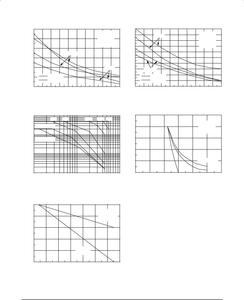
TYPICAL SWITCHING CHARACTERISTICS (IB2 = IC/2 for all switching)
|
180 |
|
|
|
|
|
|
|
|
|
|
250 |
|
|
|
|
|
|
|
|
|
IB(off) = IC/2 |
|
230 |
|
|
160 |
|
|
|
|
|
|
|
VCC = 15 V |
|
210 |
|
|
|
|
|
|
|
|
|
|
VZ = 300 V |
(ns) |
||
|
140 |
|
|
|
|
|
|
|
LC = 200 μH |
190 |
||
(ns) |
|
|
|
|
|
|
|
|
|
TIME |
170 |
|
|
|
|
|
IC = 0.4 A |
|
|
|
|
||||
FALL, TIME |
120 |
|
|
|
|
|
|
|
-OVER |
150 |
||
|
|
|
|
|
|
|
|
|
||||
100 |
|
|
|
|
|
|
|
|
|
130 |
||
|
|
|
|
|
|
|
|
IC = 1 A |
|
|||
fi |
|
|
|
|
|
|
|
|
|
CROSS |
110 |
|
t |
|
|
|
|
|
|
|
|
|
|
|
|
|
|
|
|
|
|
|
|
|
|
|
, |
|
|
|
|
TJ = 25°C |
|
|
|
|
|
|
C |
90 |
|
|
80 |
|
|
|
|
|
|
|
T |
|||
|
|
|
|
|
|
|
|
|
|
|||
|
|
|
TJ = 125°C |
|
|
|
|
|
|
|
70 |
|
|
60 |
|
|
|
|
|
|
|
|
|
|
50 |
|
5 |
6 |
7 |
8 |
9 |
10 |
11 |
12 |
13 |
14 |
15 |
|
|
|
IC = 1 A |
|
|
|
|
IB(off) = IC/2 |
|
||
|
|
|
|
|
|
VCC |
= 15 V |
|
||
|
|
|
|
|
|
|
|
VZ = 300 V |
|
|
|
|
|
|
|
|
|
|
LC = 200 μH |
|
|
|
IC = 0.4 A |
|
|
|
|
|
|
|
|
|
|
|
TJ = 25°C |
|
|
|
|
|
|
|
|
|
|
TJ = 125°C |
|
|
|
|
|
|
|
|
5 |
6 |
7 |
8 |
9 |
10 |
11 |
12 |
13 |
14 |
15 |
hFE, FORCED GAIN |
hFE, FORCED GAIN |
Figure 13. Inductive Fall Time |
Figure 14. Inductive Crossover Time |
GUARANTEED SAFE OPERATING AREA INFORMATION
|
10.00 |
|
|
50 μs |
10 μs 1 μs |
|
|
5 ms |
1 ms |
||
(AMPS) |
|
DC (MJE18002) |
|
|
|
|
|
|
|
|
|
CURRENT |
1.00 |
|
|
|
|
|
DC (MJF18002) |
|
|
|
|
|
|
|
|
|
|
, COLLECTOR |
0.10 |
|
|
|
|
|
|
|
|
|
|
C |
|
|
|
|
|
I |
|
|
|
|
|
|
0.01 |
|
|
|
|
|
10 |
|
100 |
|
1000 |
|
|
VCE, COLLECTOR±EMITTER VOLTAGE (VOLTS) |
|||
|
2.5 |
|
|
|
|
|
|
|
(AMPS) |
2.0 |
|
|
|
TC ≤ 125°C |
|
||
|
|
|
IC/IB ≥ 4 |
|
||||
|
|
|
|
LC = 500 μH |
|
|||
CURRENT |
|
|
|
|
|
|||
1.5 |
|
|
|
|
|
|
|
|
|
|
|
|
|
|
|
|
|
COLLECTOR |
1.0 |
|
|
|
|
|
|
|
0.5 |
|
|
|
V |
BE(off) |
= 0.5 V |
|
|
, |
|
|
|
|
|
|
|
|
C |
|
|
|
0 V |
|
|
|
|
I |
|
|
|
|
|
|
|
|
|
|
|
|
|
±1.5 V |
|
||
|
0 |
|
|
|
|
|
||
|
|
|
|
|
|
|
|
|
|
0 |
200 |
400 |
600 |
800 |
1000 |
1200 |
|
VCE, COLLECTOR±EMITTER VOLTAGE (VOLTS)
Figure 15. Forward Bias Safe Operating Area |
Figure 16. Reverse Bias Switching Safe |
|
Operating Area |
|
1.0 |
|
|
|
|
|
|
|
|
|
|
|
|
|
|
SECOND |
|
FACTOR |
0.8 |
|
|
|
|
|
BREAKDOWN |
|
|
|
|
|
|
|
DERATING |
|
|
0.6 |
|
|
|
|
|
|
|
|
DERATING |
|
|
|
|
|
|
|
|
0.4 |
|
|
|
|
|
|
|
|
POWER |
0.2 |
|
|
|
THERMAL |
|
|
|
|
|
|
|
DERATING |
|
|
|
|
|
|
|
|
|
|
|
|
|
|
0 |
|
|
|
|
|
|
|
|
20 |
40 |
60 |
80 |
100 |
120 |
140 |
160 |
|
|
|
TC, CASE TEMPERATURE (°C) |
|
|
|||
Figure 17. Forward Bias Power Derating
There are two limitations on the power handling ability of a transistor: average junction temperature and second breakdown. Safe operating area curves indicate IC±VCE limits of the transistor that must be observed for reliable operation; i.e., the transistor must not be subjected to greater dissipation than the curves indicate. The data of Figure 15 is based on TC = 25°C; TJ(pk) is variable depending on power level. Second breakdown pulse limits are valid for duty cycles to 10% but must be derated when TC > 25°C. Second breakdown limitations do not derate the same as thermal limitations. Allowable current at the voltages shown on Figure 15 may be found at any case temperature by using the appropriate curve on Figure 17. TJ(pk) may be calculated from the data in Figures 20 and 21. At any case temperatures, thermal limitations will reduce the power that can be handled to values less the limitations imposed by second breakdown. For inductive loads, high voltage and current must be sustained simultaneously during turn±off with the base to emitter junction reverse biased. The safe level is specified as a reverse biased safe operating area (Figure 16). This rating is verified under clamped conditions so that the device is never subjected to an avalanche mode.
Motorola Bipolar Power Transistor Device Data |
5 |