Материал: mbrf1045rev1dx
MOTOROLA
SEMICONDUCTOR TECHNICAL DATA
Order this document by MBRF1045/D
SWITCHMODE |
|
|
|
|
|
|
|
Schottky |
Power |
Rectifier |
|
|
|
MBRF1045 |
|
The SWITCHMODE Power Rectifier employs the Schottky Barrier principle in |
|
|
|
Motorola Preferred Device |
|||
a large area metal±to±silicon power diode. State±of±the±art geometry features |
|
|
|
|
|||
epitaxial construction with oxide passivation and metal overlay contact. Ideally |
|
|
|
|
|||
suited for use as rectifiers in very low±voltage, high±frequency switching power |
|
|
|
SCHOTTKY BARRIER |
|||
supplies, free wheeling diodes and polarity protection diodes. |
|
|
|
||||
|
|
|
RECTIFIER |
||||
• Highly Stable Oxide Passivated Junction |
|
|
|
|
|
||
|
|
|
|
|
10 AMPERES |
||
• Very Low Forward Voltage Drop |
|
|
|
|
|
||
|
|
|
|
|
45 VOLTS |
||
• High Junction Temperature Capability |
|
|
|
|
|
||
|
|
|
|
|
|
||
• High dv/dt Capability |
|
|
|
|
|
|
|
• Excellent Ability to Withstand Reverse Avalanche Energy |
|
|
|
|
|||
Transients |
|
|
|
|
|
|
|
• Guardring for Stress Protection |
|
|
|
|
|
|
|
• Epoxy Meets UL94, VO at 1/8″ |
|
|
|
|
|
|
|
• Electrically Isolated. No Isolation Hardware Required. |
|
|
|
|
|||
• UL Recognized File #E69369(1) |
1 |
|
|
|
2 |
|
|
|
|||||||
|
|
|
|||||
Mechanical Characteristics |
|
|
|
1 |
|||
• Case: Epoxy, Molded |
|
|
|
|
2 |
||
• Weight: 1.9 grams (approximately) |
|
|
|
|
|
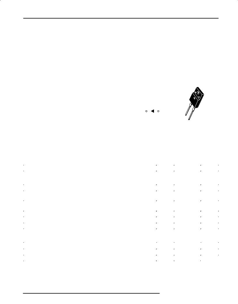
CASE 221E±01 |
|
• Finish: All External Surfaces Corrosion Resistant and Terminal |
|
|
|
ISOLATED TO±220 |
|||
Leads are Readily Solderable |
|
|
|
|
|
|
|
|
|
|
|
|
|
||
•Lead Temperature for Soldering Purposes: 260°C Max. for 10 Seconds
•Shipped 50 units per plastic tube
•Marking: B1045
MAXIMUM RATINGS
Rating |
|
Symbol |
Value |
Unit |
|
|
|
|
|
Peak Repetitive Reverse Voltage |
|
VRRM |
45 |
Volts |
Working Peak Reverse Voltage |
|
VRWM |
|
|
DC Blocking Voltage |
|
VR |
|
|
Average Rectified Forward Current (Rated VR), TC = 135°C |
|
IF(AV) |
10 |
Amps |
Peak Repetitive Forward Current |
|
IFRM |
20 |
Amps |
(Rated VR, Square Wave, 20 kHz), TC = 135°C |
|
|
|
|
Non±repetitive Peak Surge Current |
|
IFSM |
150 |
Amps |
(Surge applied at rated load conditions halfwave, single phase, 60 Hz) |
|
|
|
|
|
|
|
|
|
Peak Repetitive Reverse Surge Current (2.0 ms, 1.0 kHz) Figure 6 |
|
IRRM |
1.0 |
Amp |
Operating Junction and Storage Temperature |
|
TJ, Tstg |
± 65 to +150 |
°C |
Voltage Rate of Change (Rated VR) |
|
dv/dt |
10000 |
V/ms |
RMS Isolation Voltage (t = 1 second, R.H. ≤ 30%, T = 25°C)(2) |
Per Figure 8 |
V |
4500 |
Volts |
A |
Per Figure 9(1) |
iso1 |
|
|
|
V |
3500 |
|
|
|
|
iso2 |
|
|
|
Per Figure 10 |
Viso3 |
1500 |
|
THERMAL CHARACTERISTICS |
|
|
|
|
|
|
|
|
|
Maximum Thermal Resistance, Junction to Case |
|
RqJC |
4.0 |
°C/W |
Lead Temperature for Soldering Purposes: 1/8″ from Case for 5 seconds |
|
TL |
260 |
°C |
(1) UL Recognized mounting method is per Figure 9. |
|
|
|
|
(2) Proper strike and creepage distance must be provided. |
|
|
|
|
SWITCHMODE is a trademark of Motorola, Inc.
Preferred devices are Motorola recommended choices for future use and best overall value.
Rev 1
Rectifier Device Data
Motorola, Inc. 1996
MBRF1045
ELECTRICAL CHARACTERISTICS
Characteristic |
Symbol |
Max |
Unit |
|
|
|
|
Maximum Instantaneous Forward Voltage (3) |
vF |
|
Volts |
(iF = 20 Amp, TC = 25°C) |
|
0.84 |
|
(iF = 20 Amp, TC = 125°C) |
|
0.72 |
|
(iF = 10 Amp, TC = 125°C) |
|
0.57 |
|
Maximum Instantaneous Reverse Current (3) |
iR |
|
mA |
(Rated DC Voltage, TC = 25°C) |
|
0.1 |
|
(Rated DC Voltage, TC = 125°C) |
|
15 |
|
(3) Pulse Test: Pulse Width = 300 μs, Duty Cycle ≤ 2.0%
INSTANTANEOUS FORWARD CURRENT(AMPS) |
100 |
|
|
|
|
|
|
FORWARD CURRENT (AMPS) |
100 |
70 |
|
TJ = 150°C |
|
|
|
|
70 |
||
50 |
|
|
|
|
|
50 |
|||
30 |
|
|
|
|
|
100°C |
30 |
||
20 |
|
|
25°C |
|
|
|
20 |
||
10 |
|
|
|
|
|
10 |
|||
|
|
|
|
|
|
||||
7 |
|
|
|
|
|
|
7 |
||
5 |
|
|
|
|
|
|
5 |
||
3 |
|
|
|
|
|
|
3 |
||
2 |
|
|
|
|
|
|
2 |
||
1 |
|
|
|
|
|
|
1 |
||
0.7 |
|
|
|
|
|
|
0.7 |
||
0.5 |
|
|
|
|
|
|
0.5 |
||
0.3 |
|
|
|
|
|
|
0.3 |
||
0.2 |
|
|
|
|
|
|
0.2 |
||
0.1 |
0.4 |
0.6 |
0.8 |
1 |
1.2 |
1.4 |
0.1 |
||
0.2 |
|
||||||||
, |
|
|
|
|
|
|
|
INSTANTANEOUS, |
|
F |
|
|
vF, INSTANTANEOUS VOLTAGE (VOLTS) |
|
|
||||
i |
|
|
|
F |
|
||||
|
|
|
i |
|
|||||
|
|
TJ = 150°C |
|
|
|
|
|
|
|
|
25°C |
100°C |
|
|
|
|
|
|
|
|
0.2 |
0.4 |
0.6 |
0.8 |
1 |
1.2 |
1.4 |
|
vF, INSTANTANEOUS VOLTAGE (VOLTS) |
|
||||
I R, REVERSE CURRENT (mA)
100
10
1
0.1
0.01
0.001 0
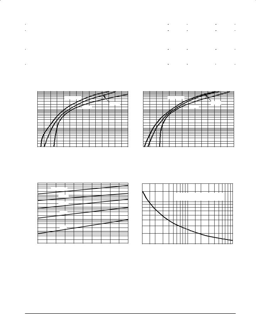
Figure 1. Maximum Forward Voltage |
Figure 2. Typical Forward Voltage |
|
|
|
|
(AMPS) |
200 |
|
|
|
|
|
|
|
|
|
|
|
TJ = 150°C |
|
|
|
|
|
|
|
|
|
|
|
|
|
|
||
|
|
|
|
|
|
|
|
|
|
|
|
|
|
|
||
|
125°C |
|
|
CURRENT |
|
|
|
|
|
TJ = 125°C, VRRM MAY BE APPLIED |
|
|
||||
|
|
|
|
100 |
|
|
|
|
BETWEEN EACH CYCLE OF SURGE |
|
|
|||||
|
|
|
|
|
|
|
|
|
|
|
||||||
|
100°C |
|
|
|
|
|
|
|
|
|
|
|
|
|
|
|
|
|
|
|
|
|
|
|
|
|
|
|
|
|
|
|
|
|
75°C |
|
|
WAVE- |
70 |
|
|
|
|
|
|
|
|
|
|
|
|
|
|
|
|
|
|
|
|
|
|
|
|
|
|
||
|
|
|
|
|
|
|
|
|
|
|
|
|
|
|
|
|
|
|
|
|
HALF |
50 |
|
|
|
|
|
|
|
|
|
|
|
|
25°C |
|
|
|
|
|
|
|
|
|
|
|
|
|
|
|
|
|
|
, PEAK |
|
|
|
|
|
|
|
|
|
|
|
|
|
|
|
|
|
30 |
|
|
|
|
|
|
|
|
|
|
|
|
|
|
|
|
FSM |
|
|
|
|
|
|
|
|
|
|
|
|
|
|
|
|
I |
20 |
|
|
|
|
|
|
|
|
|
|
|
10 |
20 |
30 |
40 |
50 |
1 |
2 |
3 |
5 |
7 |
10 |
20 |
30 |
50 |
70 |
100 |
|
|
VR, REVERSE VOLTAGE (VOLTS) |
|
|
|
|
|
|
NUMBER OF CYCLES AT 60 Hz |
|
|
|
|||||
Figure 3. Maximum Reverse Current |
Figure 4. Maximum Surge Capability |
2 |
Rectifier Device Data |
HIGH FREQUENCY OPERATION
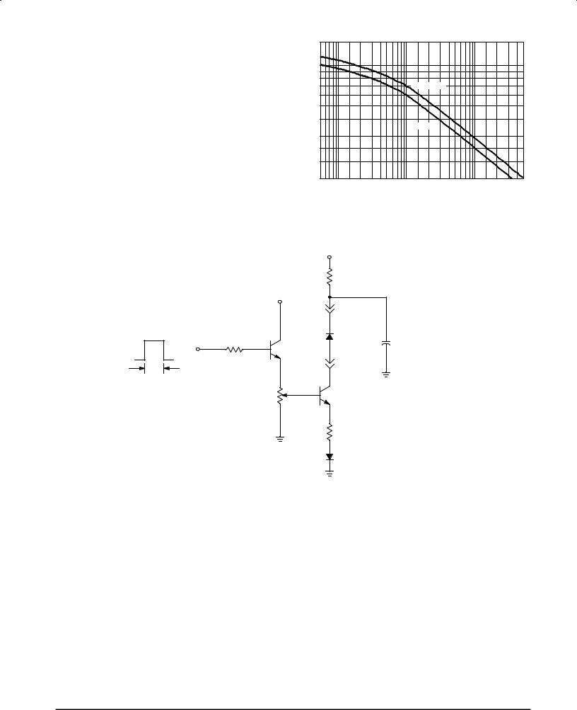
Since current flow in a Schottky rectifier is the result of majority carrier conduction, it is not subject to junction diode forward and reverse recovery transients due to minority carrier injection and stored charge. Satisfactory circuit analysis work may be performed by using a model consisting of an ideal diode in parallel with a variable capacitance. (See Figure 5.)
Rectification efficiency measurements show that operation will be satisfactory up to several megahertz. For example, relative waveform rectification efficiency is approximately 70 percent at 2.0 MHz, e.g., the ratio of dc power to RMS power in the load is 0.28 at this frequency, whereas perfect rectification would yield 0.406 for sine wave inputs. However, in contrast to ordinary junction diodes, the loss in waveform efficiency is not indicative of power loss; it is simply a result of reverse current flow through the diode capacitance, which lowers the dc output voltage.
|
|
|
|
|
|
|
|
MBRF1045 |
||
|
1500 |
|
|
|
|
|
|
|
|
|
|
1000 |
|
|
|
|
|
|
|
|
|
(pF) |
700 |
|
|
|
|
MAXIMUM |
|
|
|
|
|
|
|
|
|
|
|
|
|
|
|
CAPACITANCE |
500 |
|
|
|
|
|
|
|
|
|
|
|
|
|
|
TYPICAL |
|
|
|
|
|
300 |
|
|
|
|
|
|
|
|
|
|
C, |
|
|
|
|
|
|
|
|
|
|
|
|
|
|
|
|
|
|
|
|
|
|
200 |
|
|
|
|
|
|
|
|
|
|
150 |
0.1 |
0.2 |
0.5 |
1 |
2 |
5 |
10 |
20 |
50 |
|
0.05 |
|||||||||
|
|
|
|
VR, REVERSE VOLTAGE (VOLTS) |
|
|
||||
Figure 5. Capacitance
|
|
+150 V, 10 mAdc |
|
|
|
|
2.0 kΩ |
|
|
|
VCC |
12 Vdc |
|
|
12 V |
100 |
D.U.T. |
+ |
μF |
2N2222 |
4.0 |
|||
|
|
|
|
|
2.0 μs
1.0 kHz
CURRENT |
2N6277 |
|
AMPLITUDE |
||
100 |
||
ADJUST |
||
CARBON |
||
0 ± 10 AMPS |
||
|
1.0 CARBON
1N5817
Figure 6. Test Circuit for dv/dt and Reverse Surge Current
Rectifier Device Data |
3 |
MBRF1045
TEST CONDITIONS FOR ISOLATION TESTS*
|
MOUNTED |
|
MOUNTED |
|
MOUNTED |
|
|
CLIP |
FULLY ISOLATED |
CLIP |
FULLY ISOLATED |
|
FULLY ISOLATED |
|
|
PACKAGE |
PACKAGE |
0.107″ MIN |
PACKAGE |
0.107″ MIN |
|||
|
|
LEADS |
LEADS |
HEATSINK |
HEATSINK |
0.110″ MIN |
|
LEADS
HEATSINK |
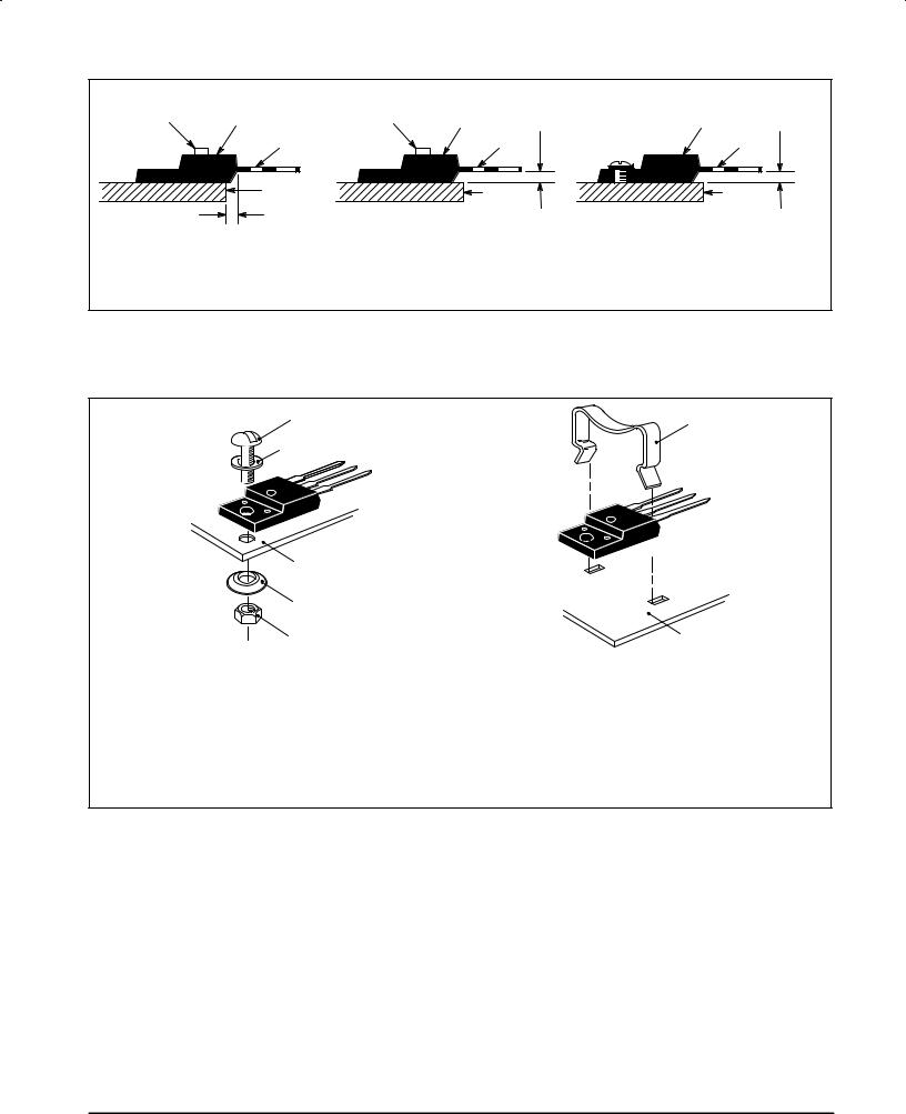
Figure 7. Clip Mounting Position |
Figure 8. Clip Mounting Position |
Figure 9. Screw Mounting Position |
for Isolation Test Number 1 |
for Isolation Test Number 2 |
for Isolation Test Number 3 |
* Measurement made between leads and heatsink with all leads shorted together.
MOUNTING INFORMATION**
4±40 SCREW |
CLIP |
PLAIN WASHER
HEATSINK
COMPRESSION WASHER
NUT |
HEATSINK |
10a. Screw±Mounted |
10b. Clip±Mounted |
Figure 10. Typical Mounting Techniques
Laboratory tests on a limited number of samples indicate, when using the screw and compression washer mounting technique, a screw torque of 6 to 8 in . lbs is sufficient to provide maximum power dissipation capability. The compression washer helps to maintain a constant pressure on the package over time and during large temperature excursions.
Destructive laboratory tests show that using a hex head 4±40 screw, without washers, and applying a torque in excess of 20 in . lbs will cause the plastic to crack around the mounting hole, resulting in a loss of isolation capability.
Additional tests on slotted 4±40 screws indicate that the screw slot fails between 15 to 20 in . lbs without adversely affecting the package. However, in order to positively ensure the package integrity of the fully isolated device, Motorola does not recommend exceeding 10 in . lbs of mounting torque under any mounting conditions.
**For more information about mounting power semiconductors see Application Note AN1040.
4 |
Rectifier Device Data |
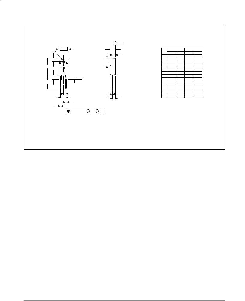
MBRF1045
PACKAGE DIMENSIONS
|
|
|
|
|
|
NOTES: |
|
|
|
|
|
|
|
|
|
±T± |
SEATING |
1. DIMENSIONING AND TOLERANCING PER ANSI |
|||||
|
|
|
|
|
Y14.5M, 1982. |
|
|
|
|||
|
|
|
|
|
PLANE |
2. |
CONTROLLING DIMENSION: INCH. |
|
|||
±B± |
|
|
C |
|
|
|
INCHES |
MILLIMETERS |
|||
F |
|
|
|
|
|
|
DIM |
MIN |
MAX |
MIN |
MAX |
|
|
|
|
S |
|
|
|||||
|
|
|
|
|
|
A |
0.621 |
0.629 |
15.78 |
15.97 |
|
Q |
|
|
|
U |
|
|
B |
0.394 |
0.402 |
10.01 |
10.21 |
|
|
|
|
|
C |
0.181 |
0.189 |
4.60 |
4.80 |
||
|
|
|
|
|
|
||||||
A |
|
|
|
|
|
|
D |
0.026 |
0.034 |
0.67 |
0.86 |
|
|
|
|
|
|
F |
0.121 |
0.129 |
3.08 |
3.27 |
|
|
|
|
|
|
|
|
G |
0.100 BSC |
2.54 BSC |
||
1 |
2 3 |
|
|
|
|
|
H |
0.123 |
0.129 |
3.13 |
3.27 |
H |
|
|
|
|
|
|
J |
0.018 |
0.025 |
0.46 |
0.64 |
±Y± |
|
|
|
|
|
K |
0.500 |
0.562 |
12.70 |
14.27 |
|
K |
|
|
|
|
|
||||||
|
|
|
|
|
L |
0.045 |
0.060 |
1.14 |
1.52 |
||
|
|
|
|
|
|
||||||
|
|
|
|
|
|
|
N |
0.200 BSC |
5.08 BSC |
||
|
|
|
|
|
|
|
Q |
0.126 |
0.134 |
3.21 |
3.40 |
|
G |
|
|
|
|
|
R |
0.107 |
0.111 |
2.72 |
2.81 |
|
|
|
J |
|
|
S |
0.096 |
0.104 |
2.44 |
2.64 |
|
|
N |
|
|
R |
|
|
U |
0.259 |
0.267 |
6.58 |
6.78 |
|
|
|
|
|
|
|
|
|
|
||
|
L |
|
|
|
|
|
|
|
|
|
|
|
|
|
|
|
|
STYLE 1: |
|
|
|
||
|
D 2 PL |
|
|
|
|
|
PIN 1. CATHODE |
|
|
||
|
|
|
|
|
|
|
2. N/A |
|
|
|
|
|
|
|
|
|
|
|
|
|
|
|
|
|
0.25 (0.010) M |
B |
M |
Y |
|
|
|
3. ANODE |
|
|
|
CASE 221E±01
ISSUE O
Rectifier Device Data |
5 |