Материал: mhpm7a15s120dc3rev0
MOTOROLA
SEMICONDUCTOR TECHNICAL DATA
Order this document by MHPM7A15S120DC3/D
Product Preview
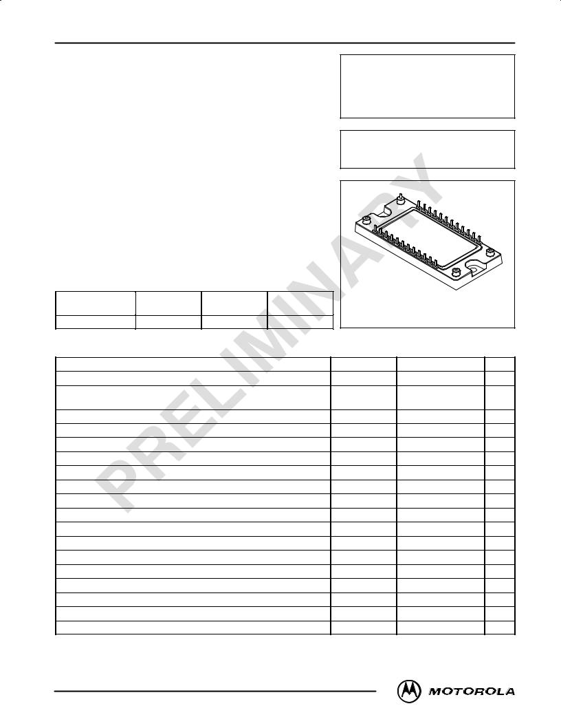
Hybrid Power Module
Integrated Power Stage for 3.0 hp 460 VAC Motor Drive
MHPM7A15S120DC3
Motorola Preferred Device
This module integrates a 3±phase inverter, 3±phase rectifier, |
|
15 AMP, 1200 VOLT |
|
|||
brake, and temperature sense in a single convenient package. It is |
|
|
||||
|
HYBRID POWER MODULE |
|
||||
designed for 3.0 hp general purpose 3±phase induction motor drive |
|
|
||||
|
|
|
||||
applications. The inverter incorporates advanced insulated gate |
|
|
|
|||
bipolar transistors (IGBT) matched with fast soft free±wheeling |
|
|
|
|||
diodes to give optimum performance. The solderable top connector |
|
|
|
|||
pins are designed for easy interfacing to the user's control board. |
|
|
|
|||
• Short Circuit Rated 10 μs @ 125°C, 720 V |
|
|
|
|
|
|
• Pin-to-Baseplate Isolation Exceeds 2500 Vac (rms) |
|
|
|
|
||
• Compact Package Outline |
|
|
|
|
|
|
• Access to Positive and Negative DC Bus |
|
|
|
|
|
|
• Independent Brake Circuit Connections |
|
|
|
|
|
|
• UL Recognition Pending |
|
|
|
|
|
|
ORDERING INFORMATION |
|
|
|
|
||
|
Voltage |
Current |
Equivalent |
|
CASE 464D±01 |
|
Device |
Rating |
Rating |
Horsepower |
|
|
|
|
ISSUE O |
|
||||
PHPM7A15S120DC3 |
1200 |
15 |
3.0 |
|
|
|
|
|
|
||||
MAXIMUM DEVICE RATINGS (TJ = 25°C unless otherwise noted) |
|
|
|
|||
|
Rating |
|
|
Symbol |
Value |
Unit |
Repetitive Peak Input Rectifier Reverse Voltage (TJ = 25°C to 150°C) |
VRRM |
900 |
V |
|||
Non±Repetitive Peak Input Rectifier Reverse Voltage (1) |
|
V |
1600 |
V |
||
(TJ = 25°C to 150°C) |
|
|
|
RSM |
|
|
|
|
|
|
|
|
|
IGBT Reverse Voltage |
|
|
|
VCES |
1200 |
V |
Gate-Emitter Voltage |
|
|
|
VGES |
± 20 |
V |
Continuous IGBT Collector Current (TC = 25°C) |
|
|
ICmax |
15 |
A |
|
Repetitive Peak IGBT Collector Current (2) |
|
|
I |
30 |
A |
|
|
|
|
|
C(pk) |
|
|
Continuous Free±Wheeling Diode Current (TC = 25°C) |
|
IFmax |
15 |
A |
||
Continuous Free±Wheeling Diode Current (TC = 80°C) |
|
IF80 |
11.7 |
A |
||
Repetitive Peak Free±Wheeling Diode Current (2) |
|
|
I |
30 |
A |
|
|
|
|
|
F(pk) |
|
|
Average Converter Output Current (Peak±to±Average ratio of 10, TC = 95°C) |
IOmax |
16 |
A |
|||
IGBT Power Dissipation per die (TC = 95°C) |
|
|
PD |
36 |
W |
|
Free±Wheeling Diode Power Dissipation per die (TC = 95°C) |
|
PD |
16 |
W |
||
Junction Temperature Range |
|
|
|
TJ |
± 40 to +150 |
°C |
Short Circuit Duration (VCE = 720 V, TJ = 125°C) |
|
|
tsc |
10 |
ms |
|
Isolation Voltage, pin to baseplate |
|
|
VISO |
2500 |
Vac |
|
Operating Case Temperature Range |
|
|
TC |
± 40 to +95 |
°C |
|
Storage Temperature Range |
|
|
|
Tstg |
± 40 to +150 |
°C |
Mounting Torque Ð Heat Sink Mounting Holes |
|
|
Ð |
12 |
lb±in |
|
(1)Half±Sine 60 Hz, maximum reverse voltage capability decreases by 0.1% per °C at lower temperature
(2)1.0 ms = 1.0% duty cycle
Preferred devices are Motorola recommended choices for future use and best overall value.
This document contains information on a product under development. Motorola reserves the right to change or discontinue this product without notice.
|
IGBT Device Data |
1 |
Motorola, Inc. 1998 |
|
|

MHPM7A15S120DC3
ELECTRICAL CHARACTERISTICS (TJ = 25°C unless otherwise noted)
Characteristic |
Symbol |
Min |
Typ |
Max |
Unit |
|
|
|
|
|
|
DC AND SMALL SIGNAL CHARACTERISTICS |
|
|
|
|
|
|
|
|
|
|
|
Input Rectifier Forward Voltage (IF = 15 A) |
VF |
Ð |
1.09 |
1.38 |
V |
Gate±Emitter Leakage Current (VCE = 0 V, VGE = ± 20 V) |
IGES |
Ð |
Ð |
±20 |
mA |
Collector±Emitter Leakage Current (VCE = 1200 V, VGE = 0 V) |
ICES |
Ð |
5.0 |
100 |
mA |
Gate±Emitter Threshold Voltage (VCE = VGE, IC = 1.0 mA) |
VGE(th) |
4.0 |
6.0 |
8.0 |
V |
Collector±Emitter Breakdown Voltage (IC = 10 mA, VGE = 0 V) |
V(BR)CES |
1200 |
Ð |
Ð |
V |
Collector±Emitter Saturation Voltage (IC = ICmax, VGE = 15 V) |
VCE(sat) |
Ð |
2.5 |
3.5 |
V |
Free±Wheeling Diode Forward Voltage (IF = IFmax, VGE = 0 V) |
VF |
1.8 |
2.0 |
2.5 |
V |
Input Capacitance (VGE = 0 V, VCE = 25 V, f = 1.0 MHz) |
Cies |
Ð |
2800 |
Ð |
pF |
Input Gate Charge (VCE = 600 V, IC = ICmax, VGE = 15 V) |
QT |
Ð |
100 |
Ð |
nC |
THERMAL CHARACTERISTICS, EACH DIE |
|
|
|
|
|
|
|
|
|
|
|
Thermal Resistance Ð IGBT |
RqJC |
Ð |
1.1 |
1.5 |
°C/W |
Thermal Resistance Ð Free±Wheeling (Fast Soft) Diode |
RqJC |
Ð |
2.4 |
3.3 |
°C/W |
Thermal Resistance Ð Input Rectifier |
RqJC |
Ð |
3.2 |
4.2 |
°C/W |
TEMPERATURE SENSE DIODE |
|
|
|
|
|
|
|
|
|
|
|
Forward Voltage (@ IF = 1.0 mA) |
VF |
1.983 |
2.024 |
2.066 |
V |
Forward Voltage Temperature Coefficient (@ IF = 1.0 mA) |
TCVF |
Ð |
±8.64 |
Ð |
mV/°C |
2 |
Motorola IGBT Device Data |
|
|
|
|
|
|
|
|
|
|
|
|
MHPM7A15S120DC3 |
|||
|
|
|
|
|
|
TYPICAL CHARACTERISTICS |
|
|
|
|
|
||||
|
30 |
|
|
|
|
|
|
|
30 |
|
|
|
|
|
|
|
27 |
|
|
|
|
TJ = 25°C |
|
|
|
|
|
|
|
|
|
(AMPS) |
|
|
|
|
|
|
(AMPS) |
25 |
|
|
|
|
|
|
|
24 |
|
|
|
|
|
|
|
|
TJ = 125°C |
|
25°C |
|
|||
|
|
|
|
|
|
|
|
|
|
|
|||||
21 |
|
|
|
|
|
|
|
|
|
|
|
||||
|
|
|
|
|
|
20 |
|
|
|
|
|
|
|||
CURRENT |
|
|
|
|
|
|
CURRENT |
|
|
|
|
|
|
||
|
|
|
|
|
|
|
|
|
|
|
|
|
|||
18 |
|
|
|
|
|
|
|
|
|
|
|
|
|
||
15 |
|
|
|
|
|
|
15 |
|
|
|
|
|
|
||
|
|
|
|
|
|
|
|
|
|
|
|
|
|
||
,FORWARD |
12 |
|
|
|
|
|
|
,FORWARD |
10 |
|
|
|
|
|
|
9.0 |
|
|
|
|
|
|
|
|
|
|
|
|
|||
|
|
|
|
|
|
|
|
|
|
|
|
|
|||
6.0 |
|
|
|
|
|
|
5.0 |
|
|
|
|
|
|
||
F |
|
|
|
|
|
|
F |
|
|
|
|
|
|
||
I |
|
|
|
|
|
|
|
I |
|
|
|
|
|
|
|
|
3.0 |
|
|
|
|
|
|
|
|
|
|
|
|
|
|
|
0 |
|
|
|
|
|
|
|
0 |
|
|
|
|
|
|
|
0 |
0.2 |
0.4 |
0.6 |
0.8 |
1.0 |
1.2 |
1.4 |
0 |
0.5 |
1.0 |
1.5 |
2.0 |
2.5 |
3.0 |
|
|
|
VF, FORWARD VOLTAGE (VOLTS) |
|
|
|
|
VF, FORWARD VOLTAGE (VOLTS) |
|
|
|||||
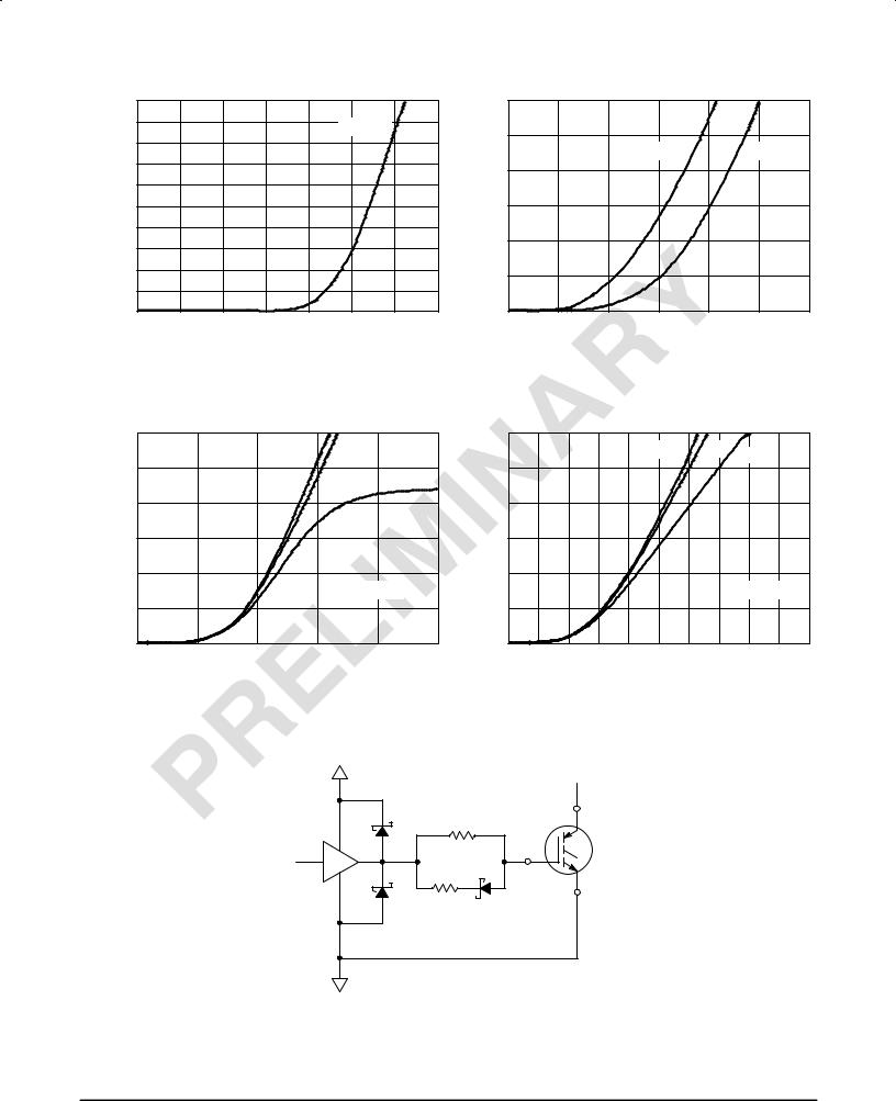
Figure 1. Forward Characteristics Ð |
Figure 2. Forward Characteristics Ð |
Input Rectifier |
Free±Wheeling Diode |
|
30 |
|
|
|
|
|
30 |
|
|
|
VGE = 18 V |
15 V |
(AMPS) |
|
|
(AMPS) |
25 |
|
|
|
12 V |
25 |
|
|
|
|
|
|
|||
|
|
|
|
|
|
||
CURRENT |
20 |
|
|
|
|
CURRENT |
20 |
15 |
|
|
|
|
15 |
||
,COLLECTOR |
10 |
|
|
|
|
, COLLECTOR |
10 |
|
|
|
|
TJ = 25°C |
|
||
5.0 |
|
|
|
|
5.0 |
||
C |
|
|
|
|
C |
||
|
|
|
|
|
|
||
I |
|
|
|
|
|
I |
|
|
0 |
|
|
|
|
|
0 |
|
0 |
1.0 |
2.0 |
3.0 |
4.0 |
5.0 |
|
|
|
VCE, COLLECTOR±TO±EMITTER VOLTAGE (VOLTS) |
|
|
|||
|
|
|
|
VGE = 18 V |
15 V |
12 V |
|
|
||
|
|
|
|
|
|
|
|
TJ = 125°C |
|
|
0 |
0.5 |
1.0 |
1.5 |
2.0 |
2.5 |
3.0 |
3.5 |
4.0 |
4.5 |
5.0 |
|
VCE, COLLECTOR±TO±EMITTER VOLTAGE (VOLTS) |
|
||||||||
Figure 3. Forward Characteristics, TJ = 25°C |
Figure 4. Forward Characteristics, TJ = 125°C |
+15 V |
|
MBRS130T3 |
|
160 W |
|
MC33153 |
|
RG(on) |
|
20 W |
|
RG(off) |
MBRS130T3 |
|
|
MBRS130T3 |
|
Figure 5. Recommended Gate Drive Circuit
Motorola IGBT Device Data |
3 |
MHPM7A15S120DC3
TYPICAL CHARACTERISTICS
+15 V
R1
12.4 kW
 A/D INPUT 14
15
VF, FORWARD VOLTAGE @ 1 mA (VOLTS)
2.5
MAXIMUM
2.0
TYPICAL
MINIMUM
1.5
1.0
TYPICAL
VF = 2.240 ± 0.00864 T
0.5MIN: 2.199 ± 0.00864 T
MAX: 2.282 ± 0.00864 T
0
0 |
20 |
40 |
60 |
80 |
100 |
120 |
140 |
160 |
T, TEMPERATURE (°C)
|
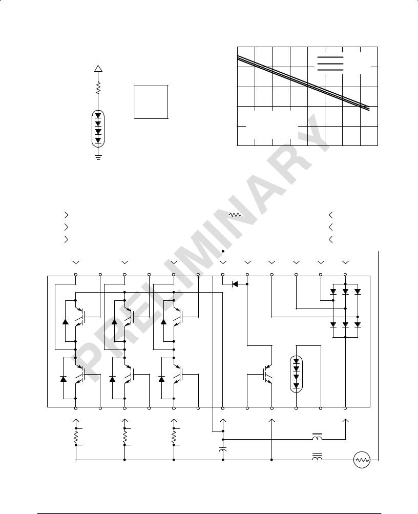
Figure 6. Recommended Temperature Sense |
|
|
Figure 7. BAV99LT1 Temperature Sense Diode |
||||||||||||||||||
|
|
|
|
Bias Circuit |
|
|
|
|
|
|
|
Performance: VF = 2.59 ± 7.31E±3 TC |
||||||||||
MOTOR OUTPUT |
|
|
|
|
|
|
|
BRAKE RESISTOR |
|
|
|
|
|
|
|
|||||||
|
|
|
|
|
|
|
|
|
|
|
|
|
|
|
|
|
||||||
U |
|
|
|
|
|
|
|
|
|
|
|
|
|
|
|
|
|
|
R |
|
|
|
|
|
|
|
|
|
|
|
|
|
|
|
|
|
|
|
|
|
|
|
|||
V |
|
|
|
|
|
|
|
|
|
|
|
|
|
|
|
|
|
|
S |
3 PHASE INPUT |
||
|
|
|
|
|
|
|
|
|
|
|
|
|
|
|
|
|
|
|||||
W |
|
|
|
|
|
|
|
|
|
|
|
|
|
|
|
|
|
|
|
T |
|
|
|
|
|
|
|
|
|
|
|
|
|
|
|
|
|
|
|
|
|
|
|||
|
|
|
|
|
|
|
|
|
|
|
|
|
|
|
|
|
|
|
|
|
|
|
|
|
|
|
|
|
|
|
|
|
|
|
|
|
|
|
|
|
|
|
|
|
|
1 |
2 |
3 |
4 |
5 |
6 |
7 |
8 |
9 |
10 |
11 |
|
12 |
||||||||||
|
|
|
|
|
|
|
|
|
|
|
|
|
|
|
|
|
|
|
|
|
|
|
|
|
|
|
|
D7 |
|
|
|
|
|
|
|
D8 |
D10 |
D12 |
D1 |
Q1 |
D3 |
Q3 |
D5 |
Q5 |
|
|
|
|
|
|
|
D9 |
D11 |
D13 |
|
|
|
|
|
TEMP |
|
|
|
|
|
|
|
SENSE |
|
|
|
|
|
|
|
D14 |
|
|
Q2 |
Q4 |
Q6 |
Q7 |
|
|||
D2 |
D4 |
D6 |
|
24 |
23 |
22 |
21 |
20 |
19 |
18 |
17 |
16 |
15 |
14 |
13 |
R1 |
|
|
|
|
|
|
|
|
|
|
FILTER |
SENSE |
|
R2 |
|
R3 |
|
|
|
|
|
|
|
|
|
|
+ |
|
|
|
|
|
|||
RESISTOR |
|
|
|
|
|
C1 |
|
|
|
R NTC |
|
|
|
|
|
|
|
|
|
|
|
||
|
|
|
|
|
|
|
|
|
|
FILTER |
|
|
|
|
|
|
|
|
|
|
|
|
Figure 8. Schematic of Module, Showing Pin±Out and
External Connections
4 |
Motorola IGBT Device Data |
MHPM7A15S120DC3
KEEP±OUT ZONES (x4)
0.585 |
0.066 |
|
0.250 |
0.175 |
|
|
0.450 |
|
1.850 |
0.925 |
0.270 |
|
|
|
0.140 |
|
|
OPTIONAL NON±PLATED |
|
|
|
|||
|
|
||||
NON±PLATED |
|
|
THRU±HOLES FOR ACCESS |
||
THRU±HOLE |
|
|
TO HEAT SINK MOUNTING |
||
|
|
|
PLATED THRU±HOLES (x24) |
|
SCREWS (x2) |
|
|
|
|
|
|
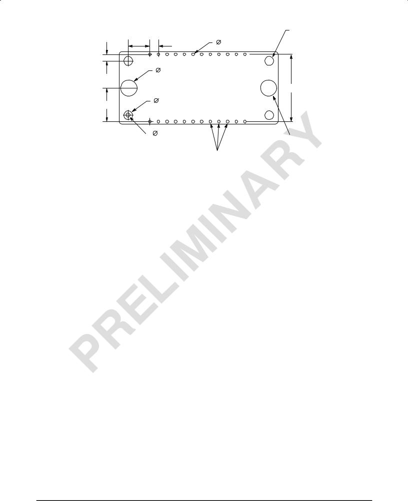
NOTES:
1.Package is symmetrical, except for a polarizing plastic post near pin 1, indicated by a non±plated thru±hole in the footprint.
2.Dimension of plated thru±holes indicates finished hole size after plating.
3.Access holes for mounting screws may or may not be necessary depending on assembly plan for finished product.
Figure 9. Package Footprint (Dimensions in Inches)
Motorola IGBT Device Data |
5 |