Материал: mmdf2c01hdrev5
MMDF2C01HD |
|
|
|
|
|
|
|
|
|
|
|
||
|
|
|
N±Channel |
|
|
|
|
|
P±Channel |
|
|
||
|
2000 |
VDS = 0 V |
|
VGS = 0 V |
|
TJ = 25°C |
|
2000 |
|
VDS = 0 V VGS = 0 V |
|
TJ = 25°C |
|
|
|
|
|
|
|
|
|
|
|||||
|
1600 |
Ciss |
|
|
|
|
|
1600 |
Ciss |
|
|
|
|
|
|
|
|
|
|
|
|
|
|
|
|||
(pF) |
|
|
|
|
|
(pF) |
|
|
|
|
|
|
|
|
|
|
|
Ciss |
|
|
|
|
|
C |
|
||
CAPACITANCEC, |
1200 |
|
|
|
|
CAPACITANCEC, |
1200 |
|
|
|
|
||
|
|
|
|
|
|
|
|
|
|
|
|
||
|
800 |
Crss |
|
|
|
|
|
800 |
Crss |
|
|
|
|
|
|
|
|
|
|
|
|
|
|
|
|||
|
|
|
|
|
|
|
|
|
|
|
|
iss |
|
|
400 |
|
|
Coss |
|
|
|
400 |
|
|
|
Coss |
|
|
|
|
|
Crss |
|
|
|
|
|
|
|
Crss |
|
|
0 |
|
|
|
|
|
|
0 |
|
|
|
|
|
|
8 |
4 |
0 |
4 |
8 |
12 |
|
8 |
4 |
0 |
4 |
8 |
12 |
VGS |
VDS |
VGS |
VDS |
GATE±TO±SOURCE OR DRAIN±TO±SOURCE VOLTAGE (VOLTS) |
GATE±TO±SOURCE OR DRAIN±TO±SOURCE VOLTAGE (Volts) |
||
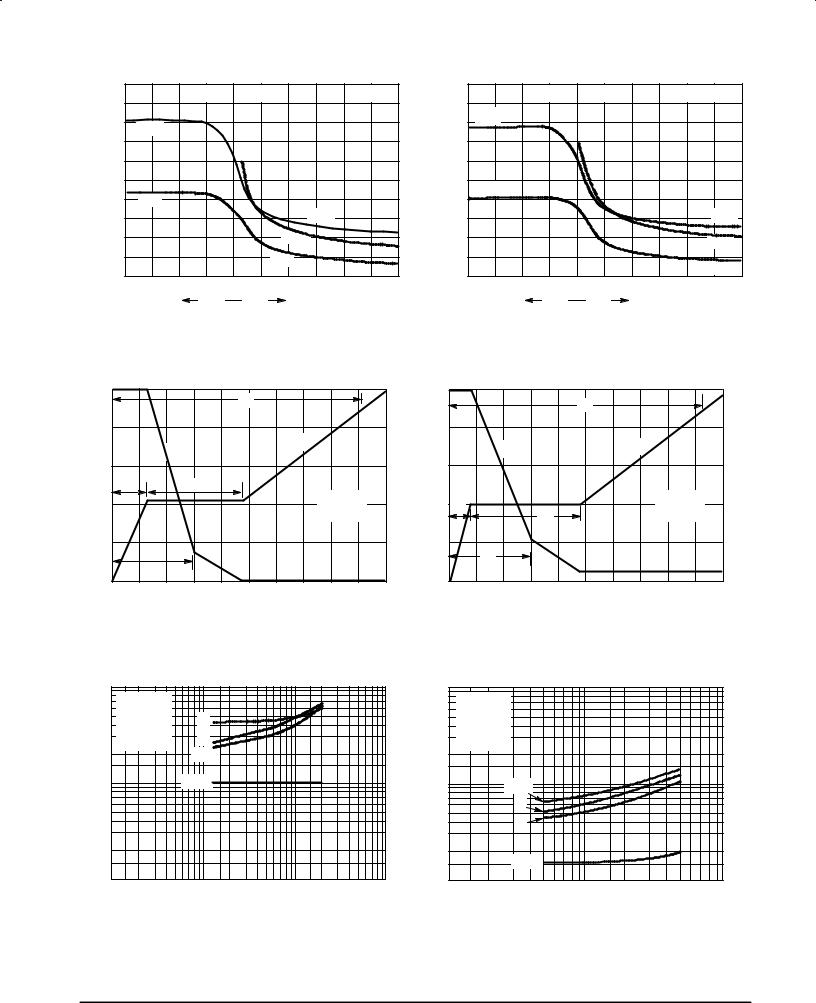
Figure 7. Capacitance Variation |
Figure 7. Capacitance Variation |
||
GATE±TO±SOURCEVOLTAGE (VOLTS) |
1 |
|
|
|
|
2 |
VOLTAGEDRAIN±TO±SOURCE, |
GATE±TO±SOURCEVOLTAGE (VOLTS) |
1 |
|
|
|
|
2 |
VOLTAGEDRAIN±TO±SOURCE, |
|
5 |
|
|
QT |
|
10 |
V |
|
5 |
|
|
|
|
10 |
V |
|
|
|
|
|
|
|
DS |
|
|
|
QT |
|
|
|
DS |
|
4 |
|
|
|
|
8 |
|
|
4 |
|
|
|
|
8 |
|
|
|
V |
|
VGS |
|
|
|
|
|
V |
|
VGS |
|
|
|
|
3 |
|
DS |
|
|
6 |
|
|
3 |
|
|
|
|
6 |
|
|
|
|
|
|
|
|
|
|
|
|
|
||||
|
Q1 |
|
Q2 |
|
|
|
|
|
|
|
|
|
|
|
|
|
2 |
|
|
|
ID = 4 A |
4 |
|
|
2 |
Q1 |
Q2 |
|
ID = 2 A |
4 |
|
|
|
|
|
|
TJ = 25°C |
|
(VOLTS) |
|
|
|
|
TJ = 25°C |
|
(VOLTS) |
|
V |
0 |
|
|
|
|
0 |
V |
0 |
|
|
|
|
0 |
||
, |
|
Q3 |
|
|
|
|
|
, |
|
Q3 |
|
|
|
|
|
GS |
|
|
|
|
|
|
|
GS |
|
|
|
|
|
|
|
|
0 |
2 |
4 |
6 |
8 |
10 |
|
|
0 |
2 |
4 |
6 |
8 |
10 |
|
|
|
|
QT, TOTAL CHARGE (nC) |
|
|
|
|
|
|
QT, TOTAL CHARGE (nC) |
|
|
|
||
Figure 8. Gate±To±Source and Drain±To±Source |
Figure 8. Gate±To±Source and Drain±To±Source |
Voltage versus Total Charge |
Voltage versus Total Charge |
t, TIME (ns)
100 |
|
|
|
|
1000 |
|
|
VDD = 6 V |
|
|
|
VDD = 6 V |
|
||
ID = 4 A |
tr |
|
|
ID = 2 A |
|
||
VGS = 4.5 V |
tf |
|
|
VGS = 4.5 V |
|
||
TJ = 25 |
° |
|
|
TJ = 25 |
° |
|
|
C |
td(off) |
|
TIME (ns) |
C |
|
||
|
|
|
|
|
|
||
10 |
|
td(on) |
|
100 |
td(off) |
|
|
|
|
|
|
t, |
|
tf |
|
|
|
|
|
|
|
|
|
|
|
|
|
|
|
tr |
|
|
|
|
|
|
|
td(on) |
|
1 |
|
|
|
|
10 |
|
|
0.1 |
|
1 |
10 |
100 |
1 |
10 |
100 |
|
|
RG, GATE RESISTANCE (OHMS) |
|
|
RG, GATE RESISTANCE (OHMS) |
|
|
Figure 9. Resistive Switching Time |
Figure 9. Resistive Switching Time |
Variation versus Gate Resistance |
Variation versus Gate Resistance |
6 |
Motorola TMOS Power MOSFET Transistor Device Data |
MMDF2C01HD
DRAIN±TO±SOURCE DIODE CHARACTERISTICS
The switching characteristics of a MOSFET body diode are very important in systems using it as a freewheeling or commutating diode. Of particular interest are the reverse recovery characteristics which play a major role in determining switching losses, radiated noise, EMI and RFI.
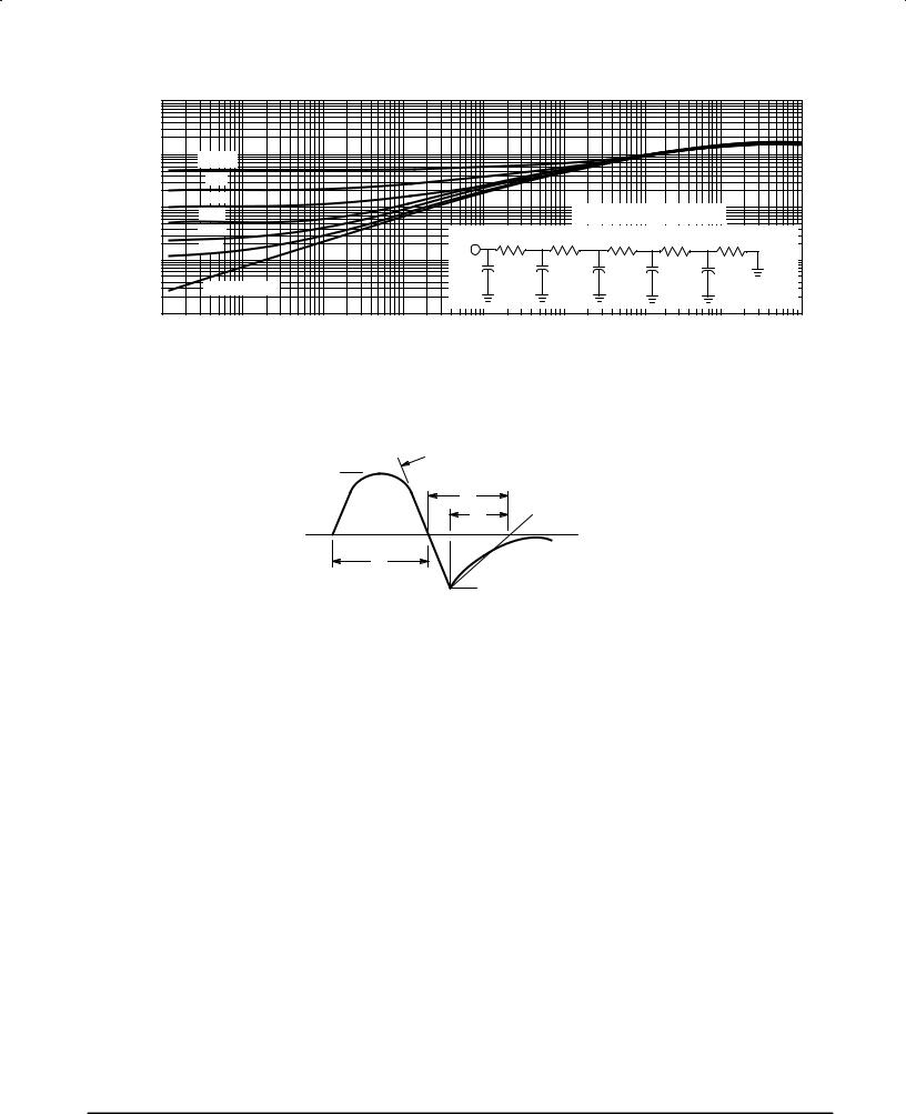
System switching losses are largely due to the nature of the body diode itself. The body diode is a minority carrier device, therefore it has a finite reverse recovery time, trr, due to the storage of minority carrier charge, QRR, as shown in the typical reverse recovery wave form of Figure 14. It is this stored charge that, when cleared from the diode, passes through a potential and defines an energy loss. Obviously, repeatedly forcing the diode through reverse recovery further increases switching losses. Therefore, one would like a diode with short trr and low QRR specifications to minimize these losses.
The abruptness of diode reverse recovery effects the amount of radiated noise, voltage spikes, and current ringing. The mechanisms at work are finite irremovable circuit parasitic inductances and capacitances acted upon by high
|
|
|
|
N±Channel |
|
|
|
|
|
4 |
|
|
|
|
|
|
|
|
|
VGS = 0 V |
|
|
|
|
|
|
(AMPS) |
|
TJ = 25°C |
|
|
|
|
|
|
3 |
|
|
|
|
|
|
|
|
|
|
|
|
|
|
|
|
|
CURRENT |
2 |
|
|
|
|
|
|
|
|
|
|
|
|
|
|
|
|
, SOURCE |
1 |
|
|
|
|
|
|
|
|
|
|
|
|
|
|
|
|
S |
|
|
|
|
|
|
|
|
I |
|
|
|
|
|
|
|
|
|
0 |
0.4 |
0.5 |
0.6 |
0.7 |
0.8 |
0.9 |
1 |
|
0.3 |
|||||||
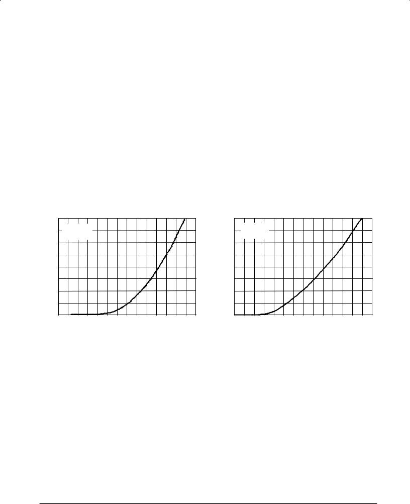
VSD, SOURCE±TO±DRAIN VOLTAGE (VOLTS)
Figure 10. Diode Forward Voltage versus Current
di/dts. The diode's negative di/dt during ta is directly controlled by the device clearing the stored charge. However, the positive di/dt during tb is an uncontrollable diode characteristic and is usually the culprit that induces current ringing. Therefore, when comparing diodes, the ratio of tb/ta serves as a good indicator of recovery abruptness and thus gives a comparative estimate of probable noise generated. A ratio of 1 is considered ideal and values less than 0.5 are considered snappy.
Compared to Motorola standard cell density low voltage MOSFETs, high cell density MOSFET diodes are faster (shorter trr), have less stored charge and a softer reverse recovery characteristic. The softness advantage of the high cell density diode means they can be forced through reverse recovery at a higher di/dt than a standard cell MOSFET diode without increasing the current ringing or the noise generated. In addition, power dissipation incurred from switching the diode will be less due to the shorter recovery time and lower switching losses.
|
|
|
|
P±Channel |
|
|
|
|
|
2 |
|
|
|
|
|
|
|
|
|
VGS = 0 V |
|
|
|
|
|
|
(AMPS) |
|
TJ = 25°C |
|
|
|
|
|
|
1.5 |
|
|
|
|
|
|
|
|
|
|
|
|
|
|
|
|
|
CURRENT |
1 |
|
|
|
|
|
|
|
|
|
|
|
|
|
|
|
|
, SOURCE |
0.5 |
|
|
|
|
|
|
|
|
|
|
|
|
|
|
|
|
S |
|
|
|
|
|
|
|
|
I |
|
|
|
|
|
|
|
|
|
0 |
0.6 |
0.8 |
1 |
1.2 |
1.4 |
1.6 |
1.8 |
|
0.4 |
|||||||
VSD, SOURCE±TO±DRAIN VOLTAGE (VOLTS)
Figure 10. Diode Forward Voltage versus Current
Motorola TMOS Power MOSFET Transistor Device Data |
7 |
MMDF2C01HD
di/dt = 300 A/μs |
Standard Cell Density |
|
trr |
CURRENT |
High Cell Density |
trr |
|
tb |
|
ta |
|
, SOURCE |
|
S |
|
I |
|
t, TIME
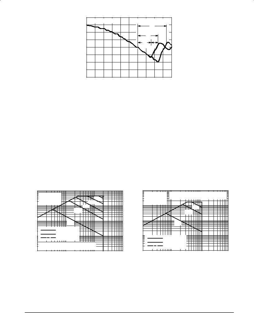
Figure 11. Reverse Recovery Time (trr)
SAFE OPERATING AREA
The Forward Biased Safe Operating Area curves define the maximum simultaneous drain±to±source voltage and drain current that a transistor can handle safely when it is forward biased. Curves are based upon maximum peak junction temperature and a case temperature (TC) of 25°C. Peak repetitive pulsed power limits are determined by using the thermal response data in conjunction with the procedures discussed in AN569, ªTransient Thermal Resistance ± General Data and Its Use.º
Switching between the off±state and the on±state may traverse any load line provided neither rated peak current (IDM) nor rated voltage (VDSS) is exceeded, and that the transition time (tr, tf) does not exceed 10 μs. In addition the total power
averaged over a complete switching cycle must not exceed
(TJ(MAX) ± TC)/(RθJC).
A power MOSFET designated E±FET can be safely used in switching circuits with unclamped inductive loads. For reliable operation, the stored energy from circuit inductance dissipated in the transistor while in avalanche must be less than the rated limit and must be adjusted for operating conditions differing from those specified. Although industry practice is to rate in terms of energy, avalanche energy capability is not a constant. The energy rating decreases non±linearly with an increase of peak current in avalanche and peak junction temperature.
N±Channel |
P±Channel |
I D , DRAIN CURRENT (AMPS)
100 |
|
|
|
VGS = 20 V |
10 μs |
|
|
SINGLE PULSE |
|
||
100 μs |
|
||
TC = 25 |
° |
|
|
C |
|
|
|
10 |
10 ms |
1 ms |
|
|
|
|
|
1 |
dc |
|
|
|
|
|
|
|
RDS(on) LIMIT |
|
|
0.1 |
THERMAL LIMIT |
|
|
PACKAGE LIMIT |
|
|
|
|
|
|
|
Mounted on 2º sq. FR4 board (1º sq. 2 oz. Cu 0.06º |
|
||
thick single sided) with one die operating, 10s max. |
|
||
0.01 |
1 |
|
|
0.1 |
10 |
100 |
|
VDS, DRAIN±TO±SOURCE VOLTAGE (VOLTS)
I D , DRAIN CURRENT (AMPS)
100 |
VGS = 8 V |
|
Mounted on 2º sq. FR4 board (1º sq. 2 oz. Cu 0.06º |
|
|
||
|
|
thick single sided) with one die operating, 10s max. |
|
|
SINGLE PULSE |
||
|
|
||
10 |
TC = 25°C |
|
|
|
|
1 ms |
|
|
|
|
|
|
|
|
10 ms |
1 |
|
|
dc |
|
|
|
|
0.1 |
|
RDS(on) LIMIT |
|
|
|
||
|
|
THERMAL LIMIT |
|
0.01 |
|
PACKAGE LIMIT |
|
|
|
|
|
0.1 |
1 |
10 |
100 |
|
VDS, DRAIN±TO±SOURCE VOLTAGE (VOLTS) |
|
|
Figure 12. Maximum Rated Forward Biased |
Figure 12. Maximum Rated Forward Biased |
Safe Operating Area |
Safe Operating Area |
8 |
Motorola TMOS Power MOSFET Transistor Device Data |
MMDF2C01HD
TYPICAL ELECTRICAL CHARACTERISTICS
|
|
10 |
|
|
|
|
|
|
|
|
|
|
Rthja(t), EFFECTIVE TRANSIENT |
THERMAL RESISTANCE |
1 |
D = 0.5 |
|
|
|
|
|
|
|
|
|
|
|
|
|
|
|
|
|
|
|
|||
|
0.2 |
|
|
|
|
|
|
|
|
|
||
0.1 |
0.1 |
|
|
|
|
Normalized to θja at 10s. |
|
|||||
0.05 |
|
|
|
|
|
|||||||
|
|
|
|
|
|
|||||||
|
0.02 |
|
|
Chip |
0.0175 Ω |
0.0710 Ω |
0.2706 Ω |
0.5776 Ω |
0.7086 Ω |
|
||
|
0.01 |
|
|
|
||||||||
|
|
|
|
|
|
|
|
|
|
|||
0.01 |
|
|
|
|
|
|
|
|
|
|
||
|
|
|
|
|
|
|
|
|
|
|
||
|
|
|
SINGLE PULSE |
|
|
|
0.0154 F |
0.0854 F |
0.3074 F |
1.7891 F |
107.55 F |
Ambient |
|
|
0.001 |
1.0E±04 |
1.0E±03 |
1.0E±02 |
1.0E±01 |
1.0E+00 |
1.0E+01 |
1.0E+02 |
1.0E+03 |
||
|
|
1.0E±05 |
||||||||||
t, TIME (s)
Figure 13. Thermal Response
di/dt |
|
IS |
|
|
trr |
ta |
tb |
|
TIME |
tp |
0.25 IS |
IS
Figure 14. Diode Reverse Recovery Waveform
Motorola TMOS Power MOSFET Transistor Device Data |
9 |
MMDF2C01HD
INFORMATION FOR USING THE SO±8 SURFACE MOUNT PACKAGE
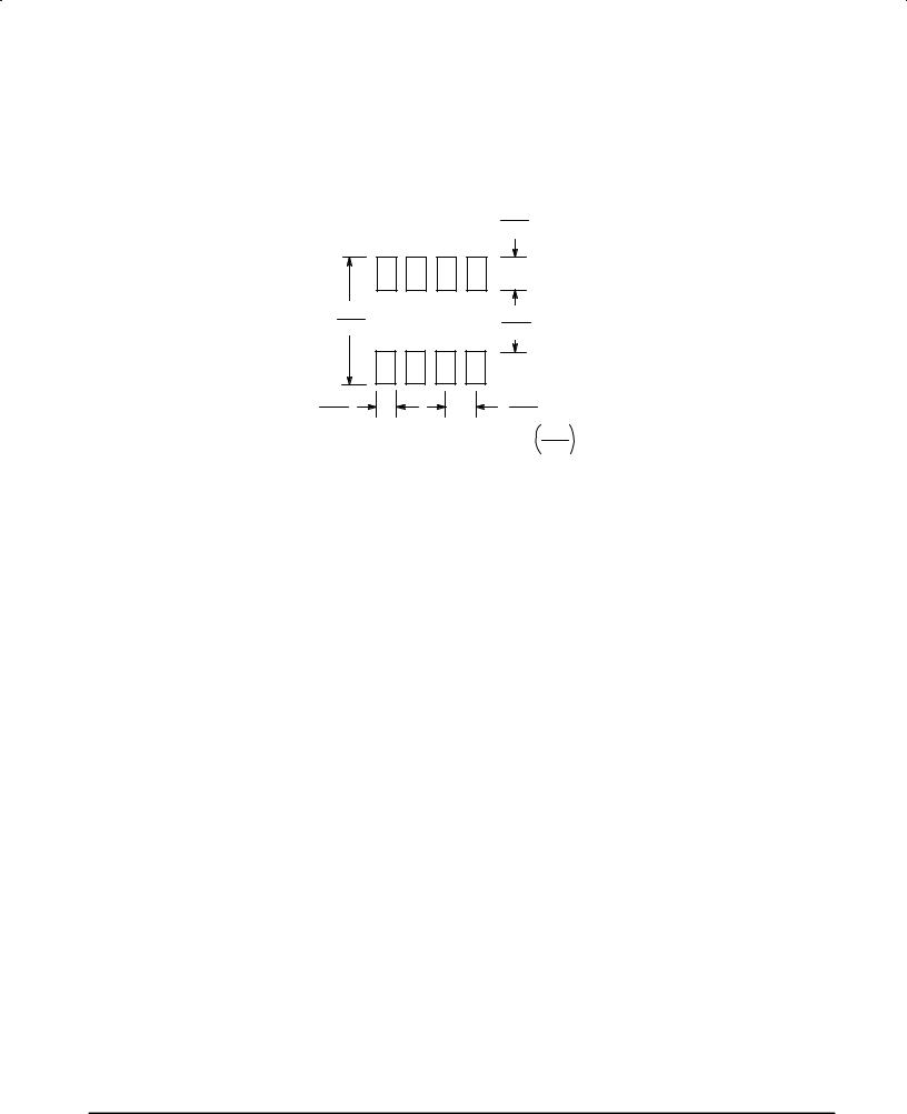
MINIMUM RECOMMENDED FOOTPRINT FOR SURFACE MOUNTED APPLICATIONS
Surface mount board layout is a critical portion of the total design. The footprint for the semiconductor packages must be the correct size to ensure proper solder connection interface
between the board and the package. With the correct pad geometry, the packages will self±align when subjected to a solder reflow process.
|
0.060 |
|
|
1.52 |
|
0.275 |
0.155 |
|
7.0 |
||
4.0 |
||
|
||
0.024 |
0.050 |
|
0.6 |
1.270 |
inches
mm
SO±8 POWER DISSIPATION
The power dissipation of the SO±8 is a function of the input pad size. This can vary from the minimum pad size for soldering to the pad size given for maximum power dissipation. Power dissipation for a surface mount device is
determined by TJ(max), the maximum rated junction temperature of the die, RθJA, the thermal resistance from the
device junction to ambient; and the operating temperature, TA. Using the values provided on the data sheet for the SO±8 package, PD can be calculated as follows:
PD = |
TJ(max) ± TA |
|
RθJA |
||
|
The values for the equation are found in the maximum ratings table on the data sheet. Substituting these values into
the equation for an ambient temperature TA of 25°C, one can calculate the power dissipation of the device which in this case is 2.0 Watts.
PD = |
150°C ± 25°C |
= 2.0 Watts |
|
62.5°C/W |
|||
|
|
The 62.5°C/W for the SO±8 package assumes the recommended footprint on a glass epoxy printed circuit board to achieve a power dissipation of 2.0 Watts using the footprint shown. Another alternative would be to use a ceramic substrate or an aluminum core board such as Thermal Clad . Using board material such as Thermal Clad, the power dissipation can be doubled using the same footprint.
SOLDERING PRECAUTIONS
The melting temperature of solder is higher than the rated temperature of the device. When the entire device is heated to a high temperature, failure to complete soldering within a short time could result in device failure. Therefore, the following items should always be observed in order to minimize the thermal stress to which the devices are subjected.
•Always preheat the device.
•The delta temperature between the preheat and soldering should be 100°C or less.*
•When preheating and soldering, the temperature of the leads and the case must not exceed the maximum temperature ratings as shown on the data sheet. When
using infrared heating with the reflow soldering method, the difference shall be a maximum of 10°C.
•The soldering temperature and time shall not exceed 260°C for more than 10 seconds.
•When shifting from preheating to soldering, the maximum temperature gradient shall be 5°C or less.
•After soldering has been completed, the device should be allowed to cool naturally for at least three minutes. Gradual cooling should be used as the use of forced cooling will increase the temperature gradient and result in latent failure due to mechanical stress.
•Mechanical stress or shock should not be applied during cooling.
* Soldering a device without preheating can cause excessive thermal shock and stress which can result in damage to the device.
10 |
Motorola TMOS Power MOSFET Transistor Device Data |