Материал: mrf1507rev1
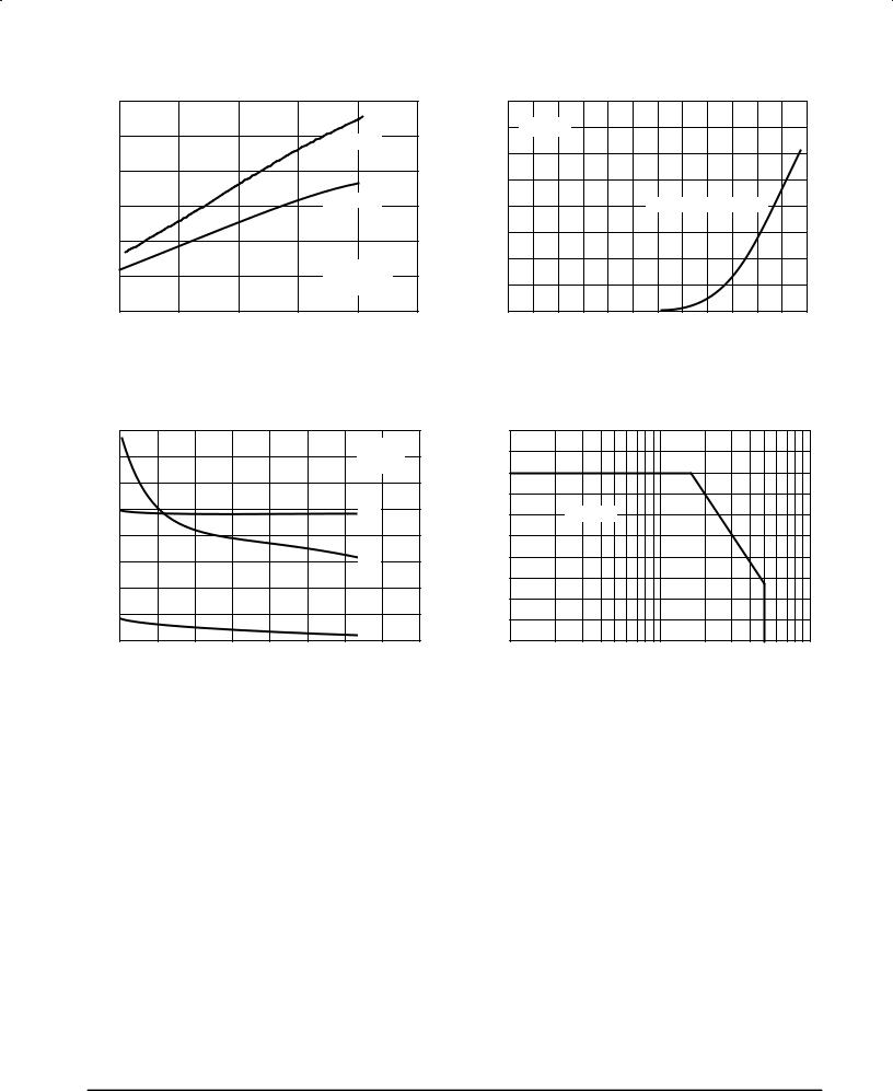
TYPICAL CHARACTERISTICS
(WATTS)POWEROUTPUT, |
17 |
|
|
|
|
(AMPS)CURRENTDRAIN |
15 |
|
|
|
VDD = 9 V |
||
|
|
|
|
|
||
|
|
|
|
|
|
|
|
13 |
|
|
|
|
|
|
11 |
|
|
|
VDD = 7.5 V |
|
out |
9 |
|
|
|
|
|
|
|
|
|
|
D |
|
P |
|
|
|
|
|
, |
7 |
|
|
|
f = 175 MHz |
I |
|
|
|
|
|
|
||
|
|
|
|
IDQ = 800 mA |
|
|
|
|
|
|
|
|
|
|
5 |
21 |
22 |
23 |
24 |
25 |
|
20 |
|||||
|
|
|
Pin, (dBm) |
|
|
|
Figure 16. Pout versus Pin
4
VDS = 10 V
3
2 |
TYPICAL DEVICE SHOWN |
1
0
0 |
1 |
2 |
3 |
4 |
5 |
6 |
|
|
VGS, GATE±SOURCE VOLTAGE (V) |
|
|
||
Figure 17. Drain Current versus Gate Voltage (Typical Device Shown)
C, CAPACITANCE (pF)
80 |
|
|
|
|
|
5 |
|
|
|
|
|
|
VGS = 0 V |
|
|
|
|
|
|
|
|
f = 1 MHz |
(AMPS) |
4 |
|
|
60 |
|
|
|
|
|
|
||
|
|
|
|
|
|
|
||
|
|
|
|
CURRENT |
|
|
|
|
|
|
|
|
Ciss |
3 |
TC = 25°C |
|
|
|
|
|
|
|
|
|||
40 |
|
|
|
|
DRAIN, |
|
|
|
|
|
|
|
Coss |
2 |
|
|
|
|
|
|
|
|
|
|
||
20 |
|
|
|
|
D |
1 |
|
|
|
|
|
|
|
I |
|
|
|
0 |
|
|
|
Crss |
|
0 |
|
|
5 |
10 |
15 |
20 |
|
10 |
100 |
||
0 |
|
0 |
||||||
|
VDS, DRAIN±SOURCE VOLTAGE (V) |
|
|
|
VDS, DRAIN±SOURCE VOLTAGE (V) |
|
||
Figure 18. Capacitance versus Voltage |
Figure 19. Maximum Rated Forward Biased |
Safe Operating Area
MRF1507 MRF1507T1 |
MOTOROLA RF DEVICE DATA |
6 |
|
f = 400 MHz |
|
|
520 |
175 |
|
ZOL* |
ZOL* |
Zo = 10 Ω |
|
||
f = 135 MHz |
f = 400 MHz |
|
520 |
Zin |
|
Zin
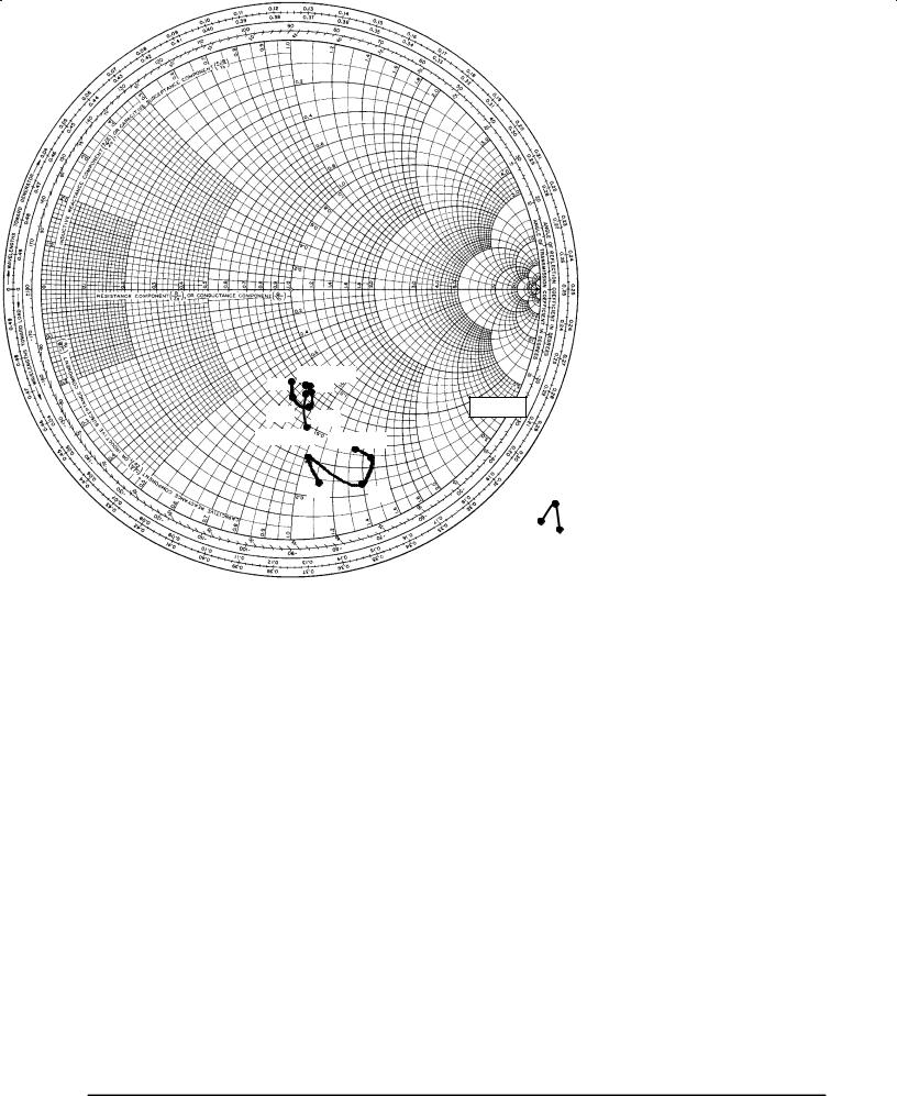
VDD = 7.5 V, IDQ = 150 mA, Pout = 8 W
f |
Zin |
ZOL* |
|
MHz |
Ω |
|
Ω |
|
|
|
|
400 |
3.6 ± j3.1 |
2.5 |
± j0.5 |
|
|
|
|
440 |
4.0 ± j3.7 |
2.7 |
± j0.6 |
|
|
|
|
470 |
3.1 ± j4.4 |
2.5 |
± j1.2 |
|
|
|
|
500 |
2.0 ± j2.71 |
2.05 |
± j0.65 |
|
|
|
|
520 |
1.9 ± j3.5 |
2.1 |
± j0.4 |
|
|
|
|
f = 135 MHz
175
VDD = 7.5 V, IDQ = 800 mA, Pout = 8 W
f |
Zin |
ZOL* |
MHz |
Ω |
Ω |
|
|
|
135 |
6.2 ± j15.1 |
2.3 ± j1.8 |
|
|
|
155 |
8.29 ± j16.9 |
2.5 ± j0.8 |
|
|
|
175 |
5.33 ± j17.0 |
2.6 ± j0.6 |
|
|
|
Zin = Conjugate of source impedance with parallel 20 Ω resistor and 82 pF capacitor in series with gate.
ZOL* = Conjugate of the load impedance at given output power, voltage, frequency, and ηD > 50 %.
Zin = |
Conjugate of source impedance with parallel |
|
10 Ω resistor and 1000 pF capacitor in series |
|
with gate. |
ZOL* = |
Conjugate of the load impedance at given |
|
output power, voltage, frequency, and ηD > 50 %. |
Note: ZOL* was chosen based on tradeoffs between gain, drain efficiency, and device stability.
MOTOROLA RF DEVICE DATA |
MRF1507 MRF1507T1 |
|
7 |

Table 1. Common Source Scattering Parameters (VDS = 7.5 Vdc)
ID = 150 mA
f |
|
S11 |
|
S21 |
S12 |
|
|
S22 |
||||
MHz |
|S11| |
|
φ |
|S21| |
|
φ |
|S12| |
|
φ |
|S22| |
|
φ |
50 |
0.76 |
|
±138 |
15.18 |
|
100 |
0.04 |
|
12 |
0.71 |
|
±141 |
|
|
|
|
|
|
|
|
|
|
|
|
|
100 |
0.77 |
|
±155 |
7.68 |
|
84 |
0.04 |
|
±3 |
0.72 |
|
±156 |
|
|
|
|
|
|
|
|
|
|
|
|
|
200 |
0.81 |
|
±162 |
3.53 |
|
65 |
0.03 |
|
±18 |
0.78 |
|
±162 |
|
|
|
|
|
|
|
|
|
|
|
|
|
300 |
0.85 |
|
±165 |
2.08 |
|
53 |
0.03 |
|
±27 |
0.83 |
|
±164 |
|
|
|
|
|
|
|
|
|
|
|
|
|
400 |
0.89 |
|
±167 |
1.37 |
|
44 |
0.03 |
|
±33 |
0.87 |
|
±166 |
|
|
|
|
|
|
|
|
|
|
|
|
|
500 |
0.91 |
|
±169 |
0.96 |
|
37 |
0.02 |
|
±36 |
0.90 |
|
±168 |
|
|
|
|
|
|
|
|
|
|
|
|
|
700 |
0.95 |
|
±171 |
0.54 |
|
27 |
0.01 |
|
±35 |
0.94 |
|
±170 |
|
|
|
|
|
|
|
|
|
|
|
|
|
850 |
0.96 |
|
±173 |
0.38 |
|
22 |
0.01 |
|
±30 |
0.95 |
|
±172 |
|
|
|
|
|
|
|
|
|
|
|
|
|
1000 |
0.97 |
|
±174 |
0.29 |
|
19 |
0.01 |
|
±19 |
0.96 |
|
±173 |
|
|
|
|
|
|
|
|
|
|
|
|
|
1200 |
0.98 |
|
±175 |
0.20 |
|
16 |
0.01 |
|
3 |
0.97 |
|
±174 |
ID = 800 mA
f |
|
S11 |
|
S21 |
S12 |
|
|
S22 |
||||
MHz |
|S11| |
|
φ |
|S21| |
|
φ |
|S12| |
|
φ |
|S22| |
|
φ |
50 |
0.82 |
|
±152 |
16.58 |
|
98 |
0.03 |
|
9 |
0.79 |
|
±161 |
|
|
|
|
|
|
|
|
|
|
|
|
|
100 |
0.81 |
|
±165 |
8.37 |
|
88 |
0.03 |
|
1 |
0.80 |
|
±169 |
|
|
|
|
|
|
|
|
|
|
|
|
|
200 |
0.82 |
|
±170 |
4.08 |
|
76 |
0.02 |
|
±8 |
0.81 |
|
±172 |
|
|
|
|
|
|
|
|
|
|
|
|
|
300 |
0.84 |
|
±172 |
2.60 |
|
68 |
0.02 |
|
±13 |
0.83 |
|
±173 |
|
|
|
|
|
|
|
|
|
|
|
|
|
400 |
0.85 |
|
±172 |
1.84 |
|
61 |
0.02 |
|
±17 |
0.84 |
|
±173 |
|
|
|
|
|
|
|
|
|
|
|
|
|
500 |
0.87 |
|
±172 |
1.38 |
|
54 |
0.02 |
|
±20 |
0.86 |
|
±173 |
|
|
|
|
|
|
|
|
|
|
|
|
|
700 |
0.90 |
|
±173 |
0.86 |
|
44 |
0.02 |
|
±21 |
0.89 |
|
±174 |
|
|
|
|
|
|
|
|
|
|
|
|
|
850 |
0.91 |
|
±174 |
0.64 |
|
38 |
0.01 |
|
±19 |
0.90 |
|
±174 |
|
|
|
|
|
|
|
|
|
|
|
|
|
1000 |
0.92 |
|
±175 |
0.49 |
|
33 |
0.01 |
|
±12 |
0.92 |
|
±175 |
|
|
|
|
|
|
|
|
|
|
|
|
|
1200 |
0.94 |
|
±176 |
0.36 |
|
29 |
0.01 |
|
2 |
0.93 |
|
±176 |
ID = 1.5 A
f |
|
S11 |
|
S21 |
S12 |
|
|
S22 |
||||
MHz |
|S11| |
|
φ |
|S21| |
|
φ |
|S12| |
|
φ |
|S22| |
|
φ |
50 |
0.83 |
|
±156 |
16.45 |
|
97 |
0.02 |
|
9 |
0.80 |
|
±164 |
|
|
|
|
|
|
|
|
|
|
|
|
|
100 |
0.83 |
|
±167 |
8.29 |
|
88 |
0.02 |
|
1 |
0.81 |
|
±171 |
|
|
|
|
|
|
|
|
|
|
|
|
|
200 |
0.83 |
|
±172 |
4.06 |
|
77 |
0.02 |
|
±6 |
0.82 |
|
±174 |
|
|
|
|
|
|
|
|
|
|
|
|
|
300 |
0.84 |
|
±173 |
2.61 |
|
70 |
0.02 |
|
±10 |
0.83 |
|
±174 |
|
|
|
|
|
|
|
|
|
|
|
|
|
400 |
0.86 |
|
±173 |
1.86 |
|
63 |
0.02 |
|
±13 |
0.85 |
|
±174 |
|
|
|
|
|
|
|
|
|
|
|
|
|
500 |
0.87 |
|
±174 |
1.41 |
|
57 |
0.02 |
|
±15 |
0.86 |
|
±174 |
|
|
|
|
|
|
|
|
|
|
|
|
|
700 |
0.89 |
|
±174 |
0.89 |
|
47 |
0.01 |
|
±16 |
0.88 |
|
±175 |
|
|
|
|
|
|
|
|
|
|
|
|
|
850 |
0.91 |
|
±175 |
0.67 |
|
41 |
0.01 |
|
±13 |
0.90 |
|
±175 |
|
|
|
|
|
|
|
|
|
|
|
|
|
1000 |
0.92 |
|
±175 |
0.52 |
|
36 |
0.01 |
|
±6 |
0.91 |
|
±175 |
|
|
|
|
|
|
|
|
|
|
|
|
|
1200 |
0.93 |
|
±176 |
0.38 |
|
31 |
0.01 |
|
8 |
0.92 |
|
±176 |
MRF1507 MRF1507T1 |
MOTOROLA RF DEVICE DATA |
8 |
|

APPLICATIONS INFORMATION
DESIGN CONSIDERATIONS
The MRF1507 is a common±source, RF power, N±Channel enhancement mode, Lateral Metal±Oxide Semiconductor Field±Effect Transistor (MOSFET). Motorola Application Note AN211A, ªFETs in Theory and Practiceº, is suggested reading for those not familiar with the construction and characteristics of FETs.
This surface mount packaged device was designed primarily for VHF and UHF portable power amplifier applications. Manufacturability is improved by utilizing the tape and reel capability for fully automated pick and placement of parts. However, care should be taken in the design process to insure proper heat sinking of the device.
The major advantages of Lateral RF power MOSFETs include high gain, simple bias systems, relative immunity from thermal runaway, and the ability to withstand severely mismatched loads without suffering damage.
MOSFET CAPACITANCES
The physical structure of a MOSFET results in capacitors between all three terminals. The metal oxide gate structure determines the capacitors from gate±to±drain (Cgd), and gate±to±source (Cgs). The PN junction formed during fabrication of the RF MOSFET results in a junction capacitance from drain±to±source (Cds). These capacitances are characterized
as input (Ciss), output (Coss) and reverse transfer (Crss) capacitances on data sheets. The relationships between the
inter±terminal capacitances and those given on data sheets are shown below. The Ciss can be specified in two ways:
1.Drain shorted to source and positive voltage at the gate.
2.Positive voltage of the drain in respect to source and zero volts at the gate.
In the latter case, the numbers are lower. However, neither method represents the actual operating conditions in RF applications.
DRAIN CHARACTERISTICS
One critical figure of merit for a FET is its static resistance in the full±on condition. This on±resistance, RDS(on), occurs in
the linear region of the output characteristic and is specified at a specific gate±source voltage and drain current. The drain±source voltage under these conditions is termed
VDS(on). For MOSFETs, VDS(on) has a positive temperature coefficient at high temperatures because it contributes to the
power dissipation within the device.
BVDSS values for this device are higher than normally required for typical applications. Measurement of BVDSS is not recommended and may result in possible damage to the device.
GATE CHARACTERISTICS
The gate of the RF MOSFET is a polysilicon material, and is electrically isolated from the source by a layer of oxide. The DC input resistance is very high ± on the order of 109 Ω Ð resulting in a leakage current of a few nanoamperes.
Gate control is achieved by applying a positive voltage to the gate greater than the gate±to±source threshold voltage,
VGS(th).
Gate Voltage Rating Ð Never exceed the gate voltage rating. Exceeding the rated VGS can result in permanent damage to the oxide layer in the gate region.
Gate Termination Ð The gates of these devices are essentially capacitors. Circuits that leave the gate open±circuited or floating should be avoided. These conditions can result in turn±on of the devices due to voltage build±up on the input capacitor due to leakage currents or pickup.
Gate Protection Ð These devices do not have an internal monolithic zener diode from gate±to±source. If gate protection is required, an external zener diode is recommended. Using a resistor to keep the gate±to±source impedance low also helps dampen transients and serves another important function. Voltage transients on the drain can be coupled to the gate through the parasitic gate±drain capacitance. If the gate±to±source impedance and the rate of voltage change on the drain are both high, then the signal coupled to the gate may be large enough to exceed the gate±threshold voltage and turn the device on.
MOTOROLA RF DEVICE DATA |
MRF1507 MRF1507T1 |
|
9 |

DC BIAS
Since the MRF1507 is an enhancement mode FET, drain current flows only when the gate is at a higher potential than the source. RF power FETs operate optimally with a quiescent drain current (IDQ), whose value is application dependent. The MRF1507 was characterized at IDQ = 150 mA, which is the suggested value of bias current for typical applications. For special applications such as linear amplification, IDQ may have to be selected to optimize the critical parameters.
The gate is a dc open circuit and draws no current. Therefore, the gate bias circuit may generally be just a simple resistive divider network. Some special applications may require a more elaborate bias system.
GAIN CONTROL
Power output of the MRF1507 may be controlled to some degree with a low power dc control signal applied to the gate, thus facilitating applications such as manual gain control, ALC/AGC and modulation systems. This characteristic is very dependent on frequency and load line.
MOUNTING
The specified maximum thermal resistance of 2°C/W assumes a majority of the 0.065″ x 0.180″ source contact on the back side of the package is in good contact with an appropriate heat sink. As with all RF power devices, the goal
of the thermal design should be to minimize the temperature at the back side of the package.
AMPLIFIER DESIGN
Impedance matching networks similar to those used with bipolar transistors are suitable for the MRF1507. For examples see Motorola Application Note AN721, ªImpedance Matching Networks Applied to RF Power Transistors.º Large± signal impedances are provided, and will yield a good first pass approximation.
Since RF power MOSFETs are triode devices, they are not unilateral. This coupled with the very high gain of the MRF1507 yields a device capable of self oscillation. Stability may be achieved by techniques such as drain loading, input shunt resistive loading, or output to input feedback. The RF test fixture implements a parallel resistor and capacitor in series with the gate, and has a load line selected for a higher efficiency, lower gain, and more stable operating region.
Two±port stability analysis with the MRF1507 S±parameters provides a useful tool for selection of loading or feedback circuitry to assure stable operation. See Motorola Application Note AN215A, ªRF Small±Signal Design Using Two±Port Parametersº for a discussion of two port network theory and stability.
MRF1507 MRF1507T1 |
MOTOROLA RF DEVICE DATA |
10 |
|