Материал: 74HC158A
MOTOROLA
SEMICONDUCTOR TECHNICAL DATA
Advance Information
Quad 2-Input Data
Selector/Multiplexer
High±Performance Silicon±Gate CMOS
The MC74HC158A is identical in pinout to the LS158. The device inputs are compatible with Standard CMOS outputs; with pullup resistors, they are compatible with LSTTL outputs.
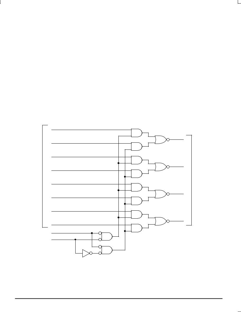
These devices route 2 nibbles (A or B) to a single port (Y) as determined by the Select input. The data is presented at the outputs in inverted form for the HC158A. A high level on the Output Enable input sets all four Y outputs to a high level for the HC158A.
•Output Drive Capability: 10 LSTTL Loads
•Outputs Directly Interface to CMOS, NMOS and TTL
•Operating Voltage Range: 2 to 6V
•Low Input Current: 1μA
•High Noise Immunity Characteristic of CMOS Devices
•In Compliance With the JEDEC Standard No. 7A Requirements
•Chip Complexity: 74 FETs or 18.5 Equivalent Gates
LOGIC DIAGRAM
|
|
A0 |
|
2 |
|
|
|
|
|
|
|
|
|
|
|
5 |
|
|
|
|
|
|
|
||
Nibble |
|
A1 |
|
|
|
|
|
|
|
|
||
|
|
11 |
|
|
|
|
|
|
|
|||
A Inputs |
|
A2 |
|
|
|
|
|
|
|
|
||
|
|
|
14 |
|
|
|
|
|
|
|
||
|
|
A3 |
|
|
|
|
|
|
|
|
||
|
|
|
|
|
|
|
|
4 |
Y0 |
|
|
|
|
|
|
|
|
|
|
|
|
|
|
||
|
|
|
|
3 |
|
|
|
7 |
|
|
||
|
|
B0 |
|
|
|
|
Y1 |
|
Data |
|||
|
|
|
|
|
|
|
||||||
|
|
|
|
|
|
9 |
|
|||||
|
|
|
6 |
|
|
|
|
|
||||
Nibble |
|
B1 |
|
|
|
|
Y2 |
|
Outputs |
|||
|
|
|
|
|
12 |
|
||||||
|
|
10 |
|
|
|
|
|
|
||||
B Inputs |
|
B2 |
|
|
|
|
Y3 |
|
|
|||
|
|
|
|
|
|
|
|
|||||
|
|
|
13 |
|
|
|
|
|
|
|
||
|
|
B3 |
|
|
|
|
|
|
|
|
||
|
|
|
|
|
|
|
|
|
|
|
|
|
|
|
|
|
|
|
|
|
|
|
|
|
|
|
|
|
|
|
|
|
|
|
|
|
|
|
|
|
Select |
1 |
|
|
Pin 16 = VCC |
|
|
||||
|
|
|
|
|
|
|||||||
|
|
|
|
|
|
Pin 8 = GND |
|
|
||||
|
|
|
|
|
|
|
|
|
|
|||
|
|
Output 15 |
|
|
|
|
|
|
|
|||
|
|
Enable |
|
|
|
|
|
|
|
|
|
|
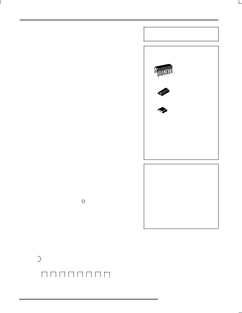
Pinout: 16±Lead Plastic Package (Top View)
MC74HC158A
|
N SUFFIX |
|
|
PLASTIC PACKAGE |
|
16 |
CASE 648±08 |
|
1 |
|
|
|
D SUFFIX |
|
16 |
SOIC PACKAGE |
|
1 |
CASE 751B±05 |
|
|
||
16 |
DT SUFFIX |
|
TSSOP PACKAGE |
||
|
||
1 |
CASE 948F-01 |
ORDERING INFORMATION
MC74HCXXXAN Plastic
MC74HCXXXAD SOIC
MC74HCXXXADT TSSOP
FUNCTION TABLE
Inputs |
Outputs |
|||||
|
|
|
|
|
|
|
Output |
Select |
|
Y0±Y3 |
|||
Enable |
|
|||||
|
|
|
|
|
|
|
|
|
|
|
|
|
|
H |
X |
|
H |
|||
L |
L |
|
|
|
|
|
|
A0±A3 |
|||||
L |
H |
|
|
|
|
|
|
B0±B3 |
|||||
|
|
|
|
|
|
|
X = Don't Care
A0±A3, B0±B3 = the levels of the respective Data±Word inputs.
|
|
|
Output |
|
|
|
|
|
|
|
|
|
|
|
|
||
VCC |
Enable |
A3 |
|
B3 |
|
Y3 |
|
A2 |
|
B2 |
|
Y2 |
|||||
|
16 |
|
|
15 |
|
14 |
|
13 |
|
12 |
|
11 |
|
10 |
|
9 |
|
|
|
|
|
|
|
|
|
|
|
|
|
|
|
|
|
|
|
|
|
|
|
|
|
|
|
|
|
|
|
|
|
|
|
|
|
|
|
|
|
|
|
|
|
|
|
|
|
|
|
|
|
|
|
1 |
|
2 |
|
3 |
|
4 |
|
5 |
|
6 |
|
7 |
|
8 |
|
Select |
A0 |
|
B0 |
|
Y0 |
|
A1 |
|
B1 |
Y1 |
GND |
||||
This document contains information on a new product. Specifications and information herein are subject to change without notice.
3/96
Motorola, Inc. 1996 |
REV 0 |
MC74HC158A
MAXIMUM RATINGS*
Symbol |
Parameter |
|
Value |
Unit |
|
|
|
|
|
||
VCC |
DC Supply Voltage (Referenced to GND) |
± 0.5 to + 7.0 |
V |
||
Vin |
DC Input Voltage (Referenced to GND) |
± 0.5 to VCC + 0.5 |
V |
||
Vout |
DC Output Voltage (Referenced to GND) |
± 0.5 to VCC + 0.5 |
V |
||
Iin |
DC Input Current, per Pin |
|
± 20 |
mA |
|
Iout |
DC Output Current, per Pin |
|
± 25 |
mA |
|
ICC |
DC Supply Current, VCC and GND Pins |
± 50 |
mA |
||
PD |
Power Dissipation in Still Air, |
Plastic DIP² |
750 |
mW |
|
|
|
SOIC Package² |
500 |
|
|
|
|
TSSOP Package² |
450 |
|
|
|
|
|
|
|
|
Tstg |
Storage Temperature |
|
± 65 to + 150 |
_C |
|
TL |
Lead Temperature, 1 mm from Case for 10 Seconds |
|
_C |
||
|
(Plastic DIP, SOIC or TSSOP Package) |
260 |
|
||
|
|
|
|
|
|
This device contains protection circuitry to guard against damage due to high static voltages or electric fields. However, precautions must be taken to avoid applications of any voltage higher than maximum rated voltages to this high±impedance circuit. For proper operation, Vin and
Vout should be constrained to the
range GND v (Vin or Vout) v VCC. Unused inputs must always be
tied to an appropriate logic voltage level (e.g., either GND or VCC). Unused outputs must be left open.
*Maximum Ratings are those values beyond which damage to the device may occur.
Functional operation should be restricted to the Recommended Operating Conditions.
²Derating Ð Plastic DIP: ± 10 mW/ _C from 65_ to 125_C
SOIC Package: ± 7 mW/_C from 65_ to 125_C
TSSOP Package: ± 6.1 mW/_C from 65_ to 125_C
For high frequency or heavy load considerations, see Chapter 2 of the Motorola High±Speed CMOS Data Book (DL129/D).
RECOMMENDED OPERATING CONDITIONS
Symbol |
Parameter |
|
Min |
Max |
Unit |
|
|
|
|
|
|
VCC |
DC Supply Voltage (Referenced to GND) |
|
2.0 |
6.0 |
V |
Vin, Vout |
DC Input Voltage, Output Voltage (Referenced to GND) |
0 |
VCC |
V |
|
TA |
Operating Temperature, All Package Types |
|
± 55 |
+ 125 |
_C |
tr, tf |
Input Rise and Fall Time |
VCC = 2.0 V |
0 |
1000 |
ns |
|
(Figure 2) |
VCC = 3.0 V |
0 |
600 |
|
|
|
VCC = 4.5 V |
0 |
500 |
|
|
|
VCC = 6.0 V |
0 |
400 |
|
DC ELECTRICAL CHARACTERISTICS (Voltages Referenced to GND)
|
|
|
|
Guaranteed Limit |
|
||
|
|
|
VCC |
|
|
|
|
|
|
|
±55_C to |
|
|
|
|
Symbol |
Parameter |
Test Conditions |
V |
25_C |
v 85_C |
v 125_C |
Unit |
|
|
|
|
|
|
|
|
VIH |
Minimum High±Level Input |
Vout = 0.1 V or VCC ± 0.1 V |
2.0 |
1.5 |
1.5 |
1.5 |
V |
|
Voltage |
|Iout| v 20 μA |
3.0 |
2.1 |
2.1 |
2.1 |
|
|
|
|
4.5 |
3.15 |
3.15 |
3.15 |
|
|
|
|
6.0 |
4.2 |
4.2 |
4.2 |
|
|
|
|
|
|
|
|
|
VIL |
Maximum Low±Level Input |
Vout = 0.1 V or VCC ± 0.1 V |
2.0 |
0.5 |
0.5 |
0.5 |
V |
|
Voltage |
|Iout| v 20 μA |
3.0 |
0.9 |
0.9 |
0.9 |
|
|
|
|
4.5 |
1.35 |
1.35 |
1.35 |
|
|
|
|
6.0 |
1.8 |
1.8 |
1.8 |
|
|
|
|
|
|
|
|
|
VOH |
Minimum High±Level Output |
Vin = VIH or VIL |
2.0 |
1.9 |
1.9 |
1.9 |
V |
|
Voltage |
|Iout| v 20 μA |
4.5 |
4.4 |
4.4 |
4.4 |
|
|
|
|
6.0 |
5.9 |
5.9 |
5.9 |
|
|
|
|
|
|
|
|
|
|
|
Vin = VIH or VIL |Iout| v 2.4 mA |
3.0 |
2.48 |
2.34 |
2.20 |
|
|
|
|Iout| v 4.0 mA |
4.5 |
3.98 |
3.84 |
3.70 |
|
|
|
|Iout| v 5.2 mA |
6.0 |
5.48 |
5.34 |
5.20 |
|
MOTOROLA |
3±2 |
MC74HC158A
DC ELECTRICAL CHARACTERISTICS (Voltages Referenced to GND)
|
|
|
|
Guaranteed Limit |
|
||
|
|
|
VCC |
|
|
|
|
|
|
|
±55_C to |
|
|
|
|
Symbol |
Parameter |
Test Conditions |
V |
25_C |
v 85_C |
v 125_C |
Unit |
|
|
|
|
|
|
|
|
VOL |
Maximum Low±Level Output |
Vin = VIH or VIL |
2.0 |
0.1 |
0.1 |
0.1 |
V |
|
Voltage |
|Iout| v 20 μA |
4.5 |
0.1 |
0.1 |
0.1 |
|
|
|
|
6.0 |
0.1 |
0.1 |
0.1 |
|
|
|
|
|
|
|
|
|
|
|
Vin = VIH or VIL |Iout| v 2.4 mA |
3.0 |
0.26 |
0.33 |
0.40 |
|
|
|
|Iout| v 4.0 mA |
4.5 |
0.26 |
0.33 |
0.40 |
|
|
|
|Iout| v 5.2 mA |
6.0 |
0.26 |
0.33 |
0.40 |
|
Iin |
Maximum Input Leakage Current |
Vin = VCC or GND |
6.0 |
± 0.1 |
± 1.0 |
± 1.0 |
μA |
ICC |
Maximum Quiescent Supply |
Vin = VCC or GND |
6.0 |
4 |
40 |
160 |
μA |
|
Current (per Package) |
Iout = 0 μA |
|
|
|
|
|
NOTE: Information on typical parametric values can be found in Chapter 2 of the Motorola High±Speed CMOS Data Book (DL129/D).
AC ELECTRICAL CHARACTERISTICS (CL = 50 pF, Input tr = tf = 6.0 ns)
|
|
|
Guaranteed Limit |
|
||
|
|
VCC |
|
|
|
|
|
|
±55_C to |
|
|
|
|
Symbol |
Parameter |
V |
25_C |
v 85_C |
v 125_C |
Unit |
|
|
|
|
|
|
|
tPLH, |
Maximum Propagation Delay, Input A to Output Y |
2.0 |
125 |
155 |
190 |
ns |
tPHL |
(Figures 1 and 4) |
3.0 |
85 |
95 |
110 |
|
|
|
4.5 |
25 |
31 |
38 |
|
|
|
6.0 |
21 |
26 |
32 |
|
|
|
|
|
|
|
|
tPLH, |
Maximum Propagation Delay, CS1 to Output Y |
2.0 |
125 |
155 |
190 |
ns |
tPHL |
(Figures 2 and 4) |
3.0 |
85 |
95 |
110 |
|
|
|
4.5 |
25 |
31 |
38 |
|
|
|
6.0 |
21 |
26 |
32 |
|
|
|
|
|
|
|
|
tPLH, |
Maximum Propagation Delay, CS2 or CS3 to Output Y |
2.0 |
115 |
145 |
175 |
ns |
tPHL |
(Figures 3 and 4) |
3.0 |
80 |
90 |
100 |
|
|
|
4.5 |
23 |
29 |
35 |
|
|
|
6.0 |
20 |
25 |
30 |
|
|
|
|
|
|
|
|
tTLH, |
Maximum Output Transition Time, Any Output |
2.0 |
75 |
95 |
110 |
ns |
tTHL |
(Figures 2 and 4) |
3.0 |
27 |
32 |
36 |
|
|
|
4.5 |
15 |
19 |
22 |
|
|
|
6.0 |
13 |
16 |
19 |
|
|
|
|
|
|
|
|
Cin |
Maximum Input Capacitance |
Ð |
10 |
10 |
10 |
pF |
NOTE: For propagation delays with loads other than 50 pF, and information on typical parametric values, see Chapter 2 of the Motorola High± Speed CMOS Data Book (DL129/D).
|
|
Typical @ 25°C, VCC = 5.0 V |
|
CPD |
Power Dissipation Capacitance (Per Package)* |
35 |
pF |
*Used to determine the no±load dynamic power consumption: PD = CPD VCC2f + ICC VCC. For load considerations, see Chapter 2 of the Motorola High±Speed CMOS Data Book (DL129/D).
3±3 |
MOTOROLA |
MC74HC158A
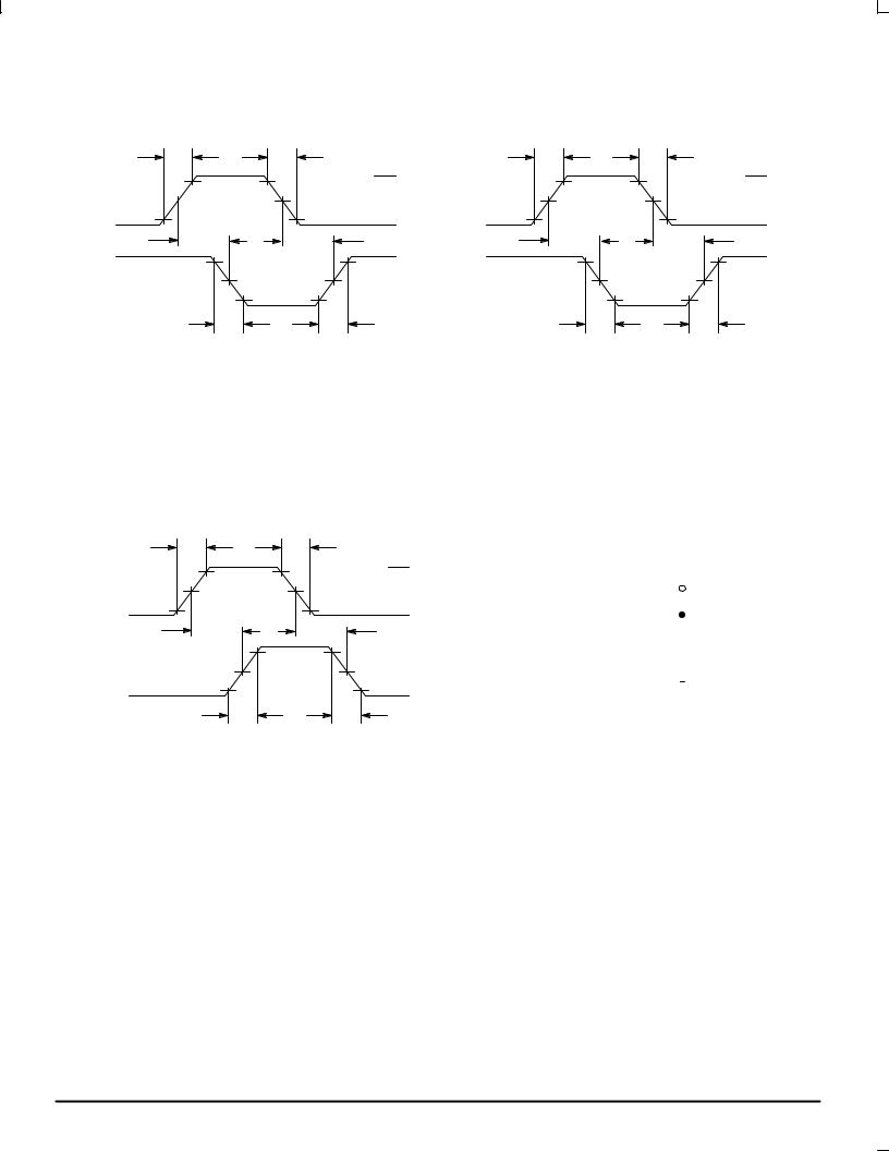
SWITCHING WAVEFORMS
tr
90%
Input Aor B |
|
50% |
|
10%
tPHL
90%
50%
Output Y
10%
tTHL
Figure 1.
tr
90%
Output Enable
50%
10%
tPLH
90%
50%
Output Y
10%
tTLH
Figure 3.
tf
VCC
GND
tPLH
tTLH
tf
VCC
GND
tPHL
tTHL
t |
|
tf |
r |
|
|
|
90% |
VCC |
Select |
50% |
|
|
10% |
GND |
|
|
|
tPHL |
|
tPLH |
|
|
90% |
Output Y |
|
50% |
|
10% |
|
|
|
|
|
t |
tTLH |
|
THL |
|
Figure 2. Y versus Select, Inverted
|
TEST |
||||||
|
POINT |
||||||
|
|
|
|
|
|
|
|
|
OUTPUT |
|
|
|
|||
DEVICE |
|
|
|
|
|
|
|
|
|
|
|
|
|
|
|
UNDER |
|
|
|
|
|
|
CL* |
TEST |
|
|
|
|
|
|
|
|
|
|
|
|
|
||
|
|
|
|
|
|
|
|
|
|
|
|
|
|
|
|
|
|
|
|
|
|
|
|
*Includes all probe and jig capacitance
Figure 4. Test Circuit
MOTOROLA |
3±4 |
MC74HC158A
PIN DESCRIPTIONS
INPUTS
A0±A3 (Pins 2,5,11,14)
Nibble A inputs. The data present on these pins is transferred to the outputs when the Select input is at a low level and the Output Enable input is at a low level. The data is presented to the outputs in inverted form for the HC158A.
B0±B3 (Pins 3,6,10,13)
Nibble B inputs. The data present on these pins is transferred to the outputs when the Select input is at a high level and the Output Enable input is at a low level. The data is presented to the outputs in inverted form for the HC158A.
OUTPUTS
Y0±Y3 (Pins 4,7,9,12)
Data outputs. The selected input nibble is presented at these outputs when the Output Enable input is at a low level.
The data present on these pins is in its inverted form for the HC158A. For the Output Enable input at a high level, the outputs are at a high level for the HC158A.
CONTROL INPUTS
Select (Pin 1)
Nibble select. This input determines the data word to be transferred to the outputs. A low level on this input selects the A inputs and a high level selects the B inputs.
Output Enable (Pin 15)
Output Enable input. A low level on thisinput allows the selected data to be presented at the outputs. A high level on this input sets all of the outputs to a high level for the HC158A.
A0 |
2 |
|
|
|
4 |
B0 |
3 |
Y0 |
|
||
A1 |
5 |
|
|
|
7 |
B1 |
6 |
Y1 |
|
||
Nibble |
|
|
Inputs |
11 |
Data |
A2 |
Outputs |
|
|
|
9 |
B2 |
10 |
Y2 |
|
||
A3 |
14 |
|
|
|
12 |
B3 |
13 |
Y3 |
|
||
Output Enable |
15 |
|
|
|
|
Select |
1 |
|
|
|
Figure 5. Expanded Logic Diagram
3±5 |
MOTOROLA |