Материал: HFA3127_
|
HFA3127 |
||
|
|
|
|
S E M I C O N D U C T O R |
|||
DESIGN INFORMATION
February 1995
Ultra High Frequency Transistor Array
The information contained in this section has been developed through characterization by Harris Semiconductor and is for use as application and design information only. No guarantee is implied.
Electrical Specifications at T |
= +25oC |
|
|
|
A |
|
|
|
|
|
|
|
|
|
PARAMETERS |
|
TEST CONDITIONS |
TYP |
UNITS |
|
|
|
|
|
Noise Figure |
|
f = 1.0GHz, VCE = 5V, IC = 5mA, ZS = 50Ω |
3.5 |
dB |
fT Current Gain-Bandwidth Product |
|
IC = 1mA, VCE = 5V |
5.5 |
GHz |
|
|
IC = 10mA, VCE = 5V |
8 |
GHz |
Power Gain-Bandwidth Product, fMAX |
|
IC = 10mA, VCE = 5V |
2.5 |
GHz |
Collector-to-Collector Leakage |
|
|
1 |
pA |
|
|
|
|
|
Collector-to-Base Capacitance |
|
0V, 1MHz |
1.6 |
pF |
|
|
|
|
|
Base-to-Emitter Capacitance |
|
0V, 1MHz |
2.2 |
pF |
|
|
|
|
|
Collector-to-Emitter Capacitance |
|
0V, 1MHz |
1.9 |
pF |
|
|
|
|
|
NOTE: Package interlead capacitance is taken into account for all capacitance measurements.
Typical Performance Curves
|
25 |
|
|
IB = 200μA |
|
(mA) |
20 |
|
|
IB = 160μA |
|
CURRENT |
15 |
|
|
IB =120μA |
|
COLLECTOR |
|
|
|
|
|
5 |
|
|
IB = 80μA |
|
|
|
10 |
|
|
|
|
|
|
|
|
IB = 40μA |
|
|
0 |
2 |
3 |
4 |
5 |
|
1 |
COLLECTOR TO EMITTER VOLTAGE (V)
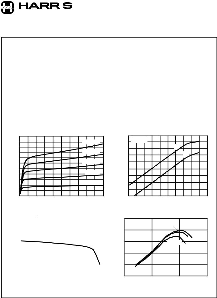
FIGURE 1. NPN COLLECTOR CURRENT vs COLLECTOR TO EMITTER VOLTAGE
|
|
|
VCE = 3V |
|
|
|
|
|
|
|
|
|
GAIN |
160 |
|
|
|
|
|
|
|
|
|
|
|
|
|
|
|
|
|
|
|
|
|
|
||
|
|
|
|
|
|
|
|
|
|
|
||
|
|
|
|
|
|
|
|
|
|
|
||
140 |
|
|
|
|
|
|
|
|
|
|
|
|
|
|
|
|
|
|
|
|
|
|
|
||
CURRENT |
80 |
|
|
|
|
|
|
|
|
|
|
|
|
120 |
|
|
|
|
|
|
|
|
|
|
|
DC |
100 |
|
|
|
|
|
|
|
|
|
|
|
60 |
|
|
|
|
|
|
|
|
|
|
|
|
|
|
|
|
|
|
|
|
|
|
|
||
|
|
|
|
|
|
|
|
|
|
|
|
|
|
40 |
|
|
|
|
|
|
|
|
|
|
|
|
|
|
|
|
|
|
|
|
|
|
|
|
|
20 |
|
|
|
|
|
|
|
|
|
|
|
|
|
|
|
|
|
|
|
|
|
|
|
|
|
0 |
|
|
|
|
|
|
|
|
|
|
|
|
1μ |
10μ |
100μ |
1m |
10m |
100m |
||||||
COLLECTOR CURRENT (A)
FIGURE 3. NPN DC CURRENT GAIN vs COLLECTOR CURRENT
|
100m |
VCE = 3V |
|
|
|
|
COLLECTORCURRENT BASEANDCURRENT (A) |
10m |
|
|
IC |
|
|
100n |
|
|
|
IB |
|
|
|
1m |
|
|
|
|
|
|
100μ |
|
|
|
|
|
|
10μ |
|
|
|
|
|
|
1μ |
|
|
|
|
|
|
10n |
|
|
|
|
|
|
1n |
|
|
|
|
|
|
0.5 |
0.6 |
0.7 |
0.8 |
0.9 |
1.0 |
BASE TO EMITTER VOLTAGE (V)
FIGURE 2. NPN COLLECTOR AND BASE CURRENTS vs BASE TO EMITTER VOLTAGE
|
10.0 |
|
|
|
(GHz) |
|
|
VCE = 3V |
|
8.0 |
|
|
|
|
PRODUCT |
|
|
|
|
|
|
|
VCE = 5V |
|
6.0 |
|
VCE = 1V |
|
|
|
|
|
||
|
|
|
|
|
BANDWIDTH |
4.0 |
|
|
|
2.0 |
|
|
|
|
GAIN |
|
|
|
|
|
|
|
|
|
|
0 |
1.0 |
10 |
100 |
|
0.1 |
|||
|
|
COLLECTOR CURRENT (mA) |
|
|
FIGURE 4. NPN GAIN BANDWIDTH PRODUCT vs COLLECTOR CURRENT (UHF 3 x 50 WITH BOND PADS)
Spec Number 511120
6
HFA3127
Ceramic Dual-In-Line Frit Seal Packages (CerDIP)
|
|
|
|
|
|
|
|
|
|
|
|
|
|
|
|
|
|
|
|
c1 |
LEAD FINISH |
|
|
|
|||||||||
|
|
|
|
|
|
|
|
|
|
|
|
|
|
|
|
|
|
|
|
|
|
|
|
|
|
|
|
|
|
|
|
|
|
|
|
|
|
|
|
-A- |
|
|
|
-D- |
|
|
|
|
|
|
|
|
|
|
|
|
|
|
|
|
|||||||
|
|
|
|
|
|
|
|
|
|
|
|
|
|
|
|
|
|
|
|
|
|
|
|
|
|
|
|
|
|
|
|
|
|
|
|
|
|
|
|
|
|
|
|
|
|
|
|
|
|
|
|
|
|
|
|
|
BASE |
|
(c) |
||||||||
|
|
|
|
|
|
|
|
|
|
|
|
|
|
|
|
E |
|
|
|
|
METAL |
|
|||||||||||
|
|
|
|
|
|
|
|
|
|
|
|
|
|
|
|
|
|
|
|
|
|
|
|||||||||||
|
|
|
|
|
|
|
|
|
|
|
|
|
|
|
|
|
|
|
|
|
|
|
|
|
|
|
|
|
|
|
|||
|
|
|
|
|
|
|
|
|
|
|
|
|
|
|
|
|
|
|
|
|
|
|
|
|
|
|
|
|
|
|
|||
|
|
|
|
|
|
|
|
|
|
|
|
|
|
|
|
|
|
|
|
|
|
|
|
b1 |
|
|
|
|
|
|
|
|
|
|
|
|
|
|
|
|
|
|
|
|
|
|
|
|
|
|
|
|
|
|
|
|
|
|
|
|
|
|
|
|
|
|
|
|
|
|
|
|
|
|
|
|
|
|
|
|
|
|
|
|
|
M |
|
|
M |
|
|
|
|
|
|
||||||
|
|
|
|
|
|
|
|
|
|
|
|
|
|
|
|
|
|
|
|
||||||||||||||
|
|
|
|
|
|
-B- |
|
|
|
|
|
|
|
|
|
|
|
|
|
|
|
(b) |
|
|
|
|
|
|
|
|
|||
|
|
|
|
|
|
|
|
|
|
|
|
|
|
|
|
|
|
|
|
|
|
SECTION A-A |
|
|
|
||||||||
|
bbb S |
C |
A - B S |
D S |
|
|
|
|
|
|
|
|
|||||||||||||||||||||
|
|
|
|
|
|
|
|
|
|
|
|
|
|
|
|
|
|
||||||||||||||||
|
|
|
|
|
|
|
|
|
|
|
|
|
|
|
|
|
|
|
|
|
|
|
|
|
|
|
|
|
|
|
|
|
|
D
BASE |
Q |
|
PLANE |
|
|
-C- |
A |
|
SEATING |
|
|
PLANE |
L |
α |
S1 |
|
eA |
A A |
|
|
b2 |
|
|
b |
e |
eA/2 |
c |
ccc M C A - B S |
D S |
aaa M C A - B S |
D S |
NOTES:
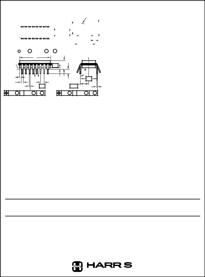
1.Index area: A notch or a pin one identification mark shall be located adjacent to pin one and shall be located within the shaded area shown. The manufacturer’s identification shall not be used as a pin one identification mark.
2.The maximum limits of lead dimensions b and c or M shall be measured at the centroid of the finished lead surfaces, when solder dip or tin plate lead finish is applied.
3.Dimensions b1 and c1 apply to lead base metal only. Dimension M applies to lead plating and finish thickness.
4.Corner leads (1, N, N/2, and N/2+1) may be configured with a partial lead paddle. For this configuration dimension b3 replaces dimension b2.
5.This dimension allows for off-center lid, meniscus, and glass overrun.
6.Dimension Q shall be measured from the seating plane to the base plane.
7.Measure dimension S1 at all four corners.
8.N is the maximum number of terminal positions.
9.Dimensioning and tolerancing per ANSI Y14.5M - 1982.
10.Controlling dimension: INCH.
F16.3 MIL-STD-1835 GDIP1-T16 (D-2, CONFIGURATION A) 16 LEAD CERAMIC DUAL-IN-LINE FRIT SEAL PACKAGE
|
INCHES |
MILLIMETERS |
|
||||
|
|
|
|
|
|
|
|
SYMBOL |
MIN |
|
MAX |
MIN |
|
MAX |
NOTES |
|
|
|
|
|
|
|
|
A |
- |
|
0.200 |
- |
|
5.08 |
- |
|
|
|
|
|
|
|
|
b |
0.014 |
|
0.026 |
0.36 |
|
0.66 |
2 |
|
|
|
|
|
|
|
|
b1 |
0.014 |
|
0.023 |
0.36 |
|
0.58 |
3 |
|
|
|
|
|
|
|
|
b2 |
0.045 |
|
0.065 |
1.14 |
|
1.65 |
- |
|
|
|
|
|
|
|
|
b3 |
0.023 |
|
0.045 |
0.58 |
|
1.14 |
4 |
|
|
|
|
|
|
|
|
c |
0.008 |
|
0.018 |
0.20 |
|
0.46 |
2 |
|
|
|
|
|
|
|
|
c1 |
0.008 |
|
0.015 |
0.20 |
|
0.38 |
3 |
|
|
|
|
|
|
|
|
D |
- |
|
0.840 |
- |
|
21.34 |
5 |
|
|
|
|
|
|
|
|
E |
0.220 |
|
0.310 |
5.59 |
|
7.87 |
5 |
|
|
|
|
|
|
||
e |
0.100 BSC |
2.54 BSC |
- |
||||
|
|
|
|
||||
eA |
0.300 BSC |
7.62 BSC |
- |
||||
|
|
|
|
||||
eA/2 |
0.150 BSC |
3.81 BSC |
- |
||||
|
|
|
|
|
|
|
|
L |
0.125 |
|
0.200 |
3.18 |
|
5.08 |
- |
|
|
|
|
|
|
|
|
Q |
0.015 |
|
0.060 |
0.38 |
|
1.52 |
6 |
|
|
|
|
|
|
|
|
S1 |
0.005 |
|
- |
0.13 |
|
- |
7 |
|
|
|
|
|
|
|
|
α |
90o |
|
105o |
90o |
|
105o |
- |
aaa |
- |
|
0.015 |
- |
|
0.38 |
- |
|
|
|
|
|
|
|
|
bbb |
- |
|
0.030 |
- |
|
0.76 |
- |
|
|
|
|
|
|
|
|
ccc |
- |
|
0.010 |
- |
|
0.25 |
- |
|
|
|
|
|
|
|
|
M |
- |
|
0.0015 |
- |
|
0.038 |
2, 3 |
|
|
|
|
|
|
|
|
N |
|
16 |
|
16 |
8 |
||
|
|
|
|
|
|
|
|
Rev. 0 4/94
Harris Semiconductor products are sold by description only. Harris Semiconductor reserves the right to make changes in circuit design and/or specifications at any time without notice. Accordingly, the reader is cautioned to verify that data sheets are current before placing orders. Information furnished by Harris is believed to be accurate and reliable. However, no responsibility is assumed by Harris or its subsidiaries for its use; nor for any infringements of patents or other rights of third parties which may result from its use. No license is granted by implication or otherwise under any patent or patent rights of Harris or its subsidiaries.
Sales Office Headquarters
For general information regarding Harris Semiconductor and its products, call 1-800-4-HARRIS
UNITED STATES |
EUROPE |
SOUTH ASIA |
NORTH ASIA |
|||
Harris Semiconductor |
Harris Semiconductor |
Harris Semiconductor H.K. Ltd. |
Harris K.K. |
|||
P. O. Box 883, Mail Stop 53-210 |
Mercure Center |
13/F Fourseas Building |
Kojimachi-Nakata Bldg. 4F |
|||
Melbourne, FL 32902 |
100, Rue de la Fusee |
208-212 Nathan Road |
5-3-5 Kojimachi |
|||
TEL: 1-800-442-7747 |
1130 Brussels, Belgium |
Tsimshatsui, Kowloon |
Chiyoda-ku, Tokyo 102 Japan |
|||
(407) 729-4984 |
TEL: (32) 2-724-2111 |
Hong Kong |
TEL: (81) |
3-3265-7571 |
||
FAX: (407) 729-5321 |
|
TEL: (852) 723-6339 |
TEL: (81) |
3-3265-7572 (Sales) |
||
|
|
|
|
|
|
|
|
|
|
|
|
|
|
S E M I C O N D U C T O R
Spec Number 511120
7