Материал: 100s1452
MOTOROLA
SEMICONDUCTOR TECHNICAL DATA
Product Preview |
|
AutoBahn Support Device |
MC100SX1452 |
(ABSD) |
|
|
|
The ABSD is a bi±directional repeater for use in a serial AutoBahn databus environment. It is a completely asynchronous part. No clock will be used.
During data transmission via the serial system bus, the ABSD receives data from the serial system bus and transmits the data to the receiving AutoBahn. Vice versa, the ABSD transmits data from the AutoBahn on the local side to the serial system bus.
The direction of the transmission is automatically determined by the activities at the serial bus I/O's.
The ABSD is able to handle a data collision, but no collision detect is provided.
A disable pin, which will be controlled by the AutoBahn board, supports the live insertion function. Enabling the ABSD requires a deassertion of the disable signal and a cutoff state at the serial system bus.
•Bi±Directional Data Transmission Up to 1600MBit/s
•8±Pin CLCC Package
•Differential Data I/Os
•Enables Live Insertion
•Self±Detecting Transmission Direction
•Enables Up to 21 Nodes
•Impedance Controlled Termination
AUTOBAHN
SUPPORT DEVICE
ABSD
FI SUFFIX
CERAMIC CLCC PACKAGE
CASE TBD
The ABSD supports variable data transfer rates of 400Mbit/s, 800Mbit/s and 1600Mbit/s. This enables the usage in combination with all AutoBahn Spanceiver components.
The ABSD will be used either as an active impedance controlled access node to a serial bus system, or it will act as a cable driver or line repeater.
Motorola's MOSAIC V process allows high speed designs up to 3GHz. The design is implemented with a flow±through pinout architecture.
The ABSD chip works from a single +5V supply.
|
EN |
|
|
TX±DRIVER |
|
LOCAL |
DIRECTION |
SER |
|
|
|
LOCAL |
CONTROL |
SER |
|
||
|
VCC |
|
|
EN |
|
|
RX±DRIVER |
|
DISABLE |
RESET |
POWER UP |
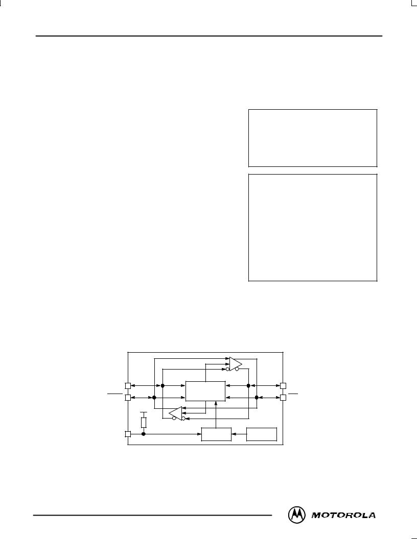
Figure 1. Simplified Block Diagram
AutoBahn and Spanceiver are trademarks of PEP Modular Computers. `Spanceiver' has been formed as a contraction of Serial/Parallel Transceiver.
MOSAIC V is a trademark of Motorola, Inc.
This document contains information on a product under development. Motorola reserves the right to change or discontinue this product without notice.
6/97
Motorola, Inc. 1997 |
1 |
REV 0 |

MC100SX1452
Table 1. PIN DESCRIPTIONS
Signal |
Pin No |
Direction |
Level |
Description |
|
|
|
|
|
DISABLE |
3 |
In |
PCT |
Low level immediately enables the ABSD if the public bus is in cutoff. High level |
|
|
|
|
disables the ABSD |
|
|
|
|
|
SER |
6 |
I/O |
CUTOFF±PECL |
Serial data I/O at the serial system bus |
|
|
|
|
|
SER |
5 |
I/O |
CUTOFF±PECL |
Inverted serial data I/O at the serial system bus |
|
|
|
|
|
LOCAL |
1 |
I/O |
CUTOFF±PECL |
Serial data I/O connected to the local AutoBahn serial bus |
|
|
|
|
|
LOCAL |
2 |
I/O |
CUTOFF±PECL |
Inverted serial data I/O connected to the local AutoBahn serial bus |
|
|
|
|
|
Power and Ground Pins |
|
|
|
|
|
|
|
|
|
GND |
4 |
Supply |
± |
Ground |
|
|
|
|
|
VCC |
8 |
Supply |
± |
Positive supply |
|
|
|
|
|
VCCO |
7 |
Supply |
± |
Positive supply output drivers |
|
|
|
|
|
BLOCK DIAGRAM FUNCTIONAL DESCRIPTION
MODES OF OPERATION
IDLE MODE
When RESET is active, both the RX±DRIVER and the TX±DRIVER are in cutoff. After enabling the part, the DRIVERs remain in cutoff state if there is no activity on the local and the public bus. If there is a data transfer running on the public bus after enabling the part, the ABSD switches to RECEIVE MODE.
RECEIVE MODE
COLLISION DETECT
In the idle mode, when DIRECTION CONTROL recognizes data on the local side and on the public side at the same time, the ABSD goes to RECEIVE MODE. The signals on the SER/SER bus (back plane) are not disturbed. On the local bus a data±collision occurs and the local AutoBahn Spanceiver shows an error.
POWER UP LOGIC
When the voltage drops below 4.6V an internal RESET± signal is generated.
RESET±LOGIC
In the idle mode, when DIRECTION CONTROL recognizes data on the public side, the ABSD switches to RECEIVE MODE. This means the RX±DRIVER becomes active and the TX±DRIVER remains in cutoff±state.
Both buffers remain in their states until the public bus goes to a cutoff state. Then the RX±DRIVER is deasserted again and the logic returns to idle mode.
The DISABLE signal indicates to the ABSD the disconnection of the local AutoBahn Spanceiver or board from the back plane, e.g., during a self test or plug/unplug of the board.
The DISABLE or the internal generated power up reset sets the internal logic to a known state. The RX±DRIVER and the TX±DRIVER are set to cutoff state. The DISABLE pin is terminated internally with a pull up resistor.
TRANSMIT MODE
In the idle mode, when DIRECTION CONTROL recognizes data on the local, side the ABSD switches to TRANSMIT MODE. This means the TX±DRIVER becomes active and the RX±DRIVER remains in cutoff±state.
Both buffers remain in their states until the local bus goes to a cutoff state. Then the TX±DRIVER is deasserted again and the logic returns to idle mode.
TX±DRIVER
The TX±DRIVER is a cutoff driver. The DIRECTION CONTROL circuit monitors the local bus. When a stable differential signal is detected the TX±DRIVER is enabled.
RX±DRIVER
The RX±DRIVER is a cutoff driver. The DIRECTION CONTROL circuit monitors the public bus. When a stable differential signal is detected the RX±DRIVER is enabled.
MOTOROLA |
2 |
ECLinPS and ECLinPS Lite |
|
|
DL140 Ð Rev 3 |
MC100SX1452
SERIAL BUS IO CHARACTERISTICS
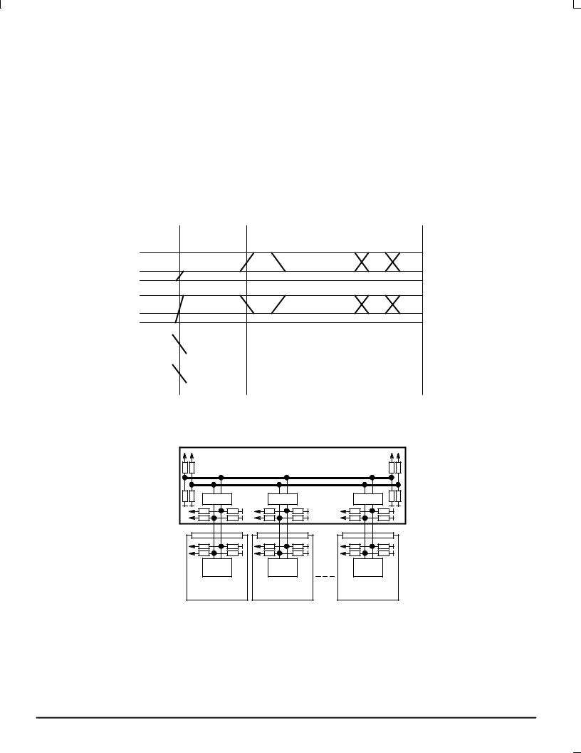
To achieve best multipoint performance the serial IO's have lowest output impedance during transmit mode and high input impedance in receive mode.
If the serial IO's are in a cutoff mode the DC input impedance is above 10KΩ. During transmit mode (differential) the IO's show a output impedance of 6Ω ± 8Ω.
TYPICAL SERIAL BUS APPLICATION
The ABSD is a bi±directional repeater for the serial
AutoBahn databus. It is a completely asynchronous part. No clock will be used.
During data transmission via the serial system bus, the ABSD receives data from the serial system bus and transmits these data to the receiving AutoBahn. Vice versa, the ABSD transmits data from the AutoBahn on the local side to the serial system bus.
The direction of the transmission is determined by the activities at the serial bus I/O's.
The ABSD is able to handle a data collision, but no collision detect is provided.
|
|
CUTOFF |
|
|
START UP PULSE |
|
|
DIFFERENTIAL DATA |
|
|
|
||||
|
|
|
|
|
|
|
|
|
|
VOH |
|
|
|
||
SERI/O |
|
VCUT |
|
|
VOL |
|
S |
|
|
S |
|
|
|
||
|
|
|
|
|
|
|
|
|
|
VOL |
|
|
|
||
|
|
|
|
|
|
|
|
|
|
|
|
|
|||
|
|
|
|
|
|
|
|
S |
|
|
S |
|
|
|
|
SERI/O |
|
VCUT |
|
|
VOH |
|
|
|
|
|
|
||||
|
|
|
|
|
|
|
|
|
|
|
|
|
|
||
|
|
|
|
|
|
|
|
|
|
|
|
|
|
||
SERI/O |
|
>10kΩ |
|
|
|
|
|
Ω |
|
|
|
||||
|
|
|
|
|
|
|
|
|
|
6±8 |
|
|
|
|
|
|
|
|
|
|
|
|
|
|
|
|
|
|
|
||
|
|
|
>10kΩ |
|
|
|
|
|
|
|
|
|
|||
SERI/O |
|
|
|
|
|
|
Ω |
|
|
|
|||||
|
|
|
|
|
|
|
|
|
|
6±8 |
|
|
|
|
|
Figure 2. Output Driver Characteristics ± Serial I/O
(LOCAL and SER)
|
|
Backplane |
|
public bus |
|
ABSD |
ABSD |
ABSD |
local bus |
local bus |
local bus |
SX1451 |
SX1451 |
SX1451 |
Board 1 |
Board 2 |
Board n |
Figure 3. Serial Bus Application
ECLinPS and ECLinPS Lite |
3 |
MOTOROLA |
DL140 Ð Rev 3 |
|
|
MC100SX1452
DISABLE
SER
SER
LOCAL
LOCAL
Receive Mode 1
DISABLE
SER
SER
LOCAL
LOCAL
Receive Mode 2
DISABLE
SER
SER
LOCAL
LOCAL
Receive Mode 3
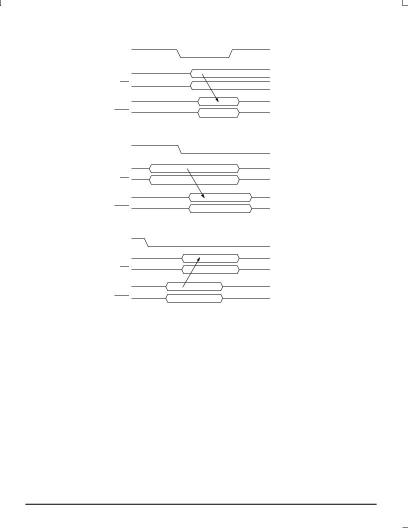
Figure 4. Functional Timings
MOTOROLA |
4 |
ECLinPS and ECLinPS Lite |
|
|
DL140 Ð Rev 3 |
MC100SX1452
|
|
|
|
|
|
|
|
|
+5V |
|
|
|
|
|
|
|
|
33pF |
83Ω |
|
|
|
+5V |
+5V |
|
Ω |
|
83Ω |
|
|
|
|
50 |
TRANSMISSION LINE |
|
||||
|
|
|
|
|
|
|
|||
|
|
|
|
|
121Ω |
121Ω |
33pF |
||
|
|
|
|
VCC |
|
|
|
|
|
|
|
|
|
|
|
|
|
|
|
|
|
|
|
VCCO |
SER |
|
|
MINIMUM DISTANCE TO |
|
|
|
|
|
ABSD |
|
|
PUBLIC SERIAL BUS |
||
|
|
|
|
SER |
|
|
|
|
|
|
|
|
|
DISABLE |
|
|
|
|
|
TO |
|
|
|
LOCAL |
|
|
|
|
+5V |
AUTOBAHN |
|
|
|
GND |
|
|
|||
|
|
|
|
|
|
|
|||
BOARD |
|
|
|
LOCAL |
|
|
|
||
|
|
|
|
|
|
|
|
||
|
Connector |
|
|
50Ω TERMINATION OF |
|
|
|
83Ω |
83Ω |
|
83Ω |
121Ω |
33pF |
|
|
|
|
||
|
|
LOCAL SERIAL BUS |
|
|
|
|
|||
|
|
|
|
|
|
|
|
||
|
+5V |
|
83Ω |
121Ω |
|
|
|
|
|
|
|
|
121Ω |
|
|
121Ω |
|
||
|
|
33pF |
+5V |
|
|
|
|
||
|
|
|
|
|
|
|
|
||
|
|
|
33pF |
|
|
|
33pF |
|
|
|
|
|
|
|
|
|
|
||
|
|
|
|
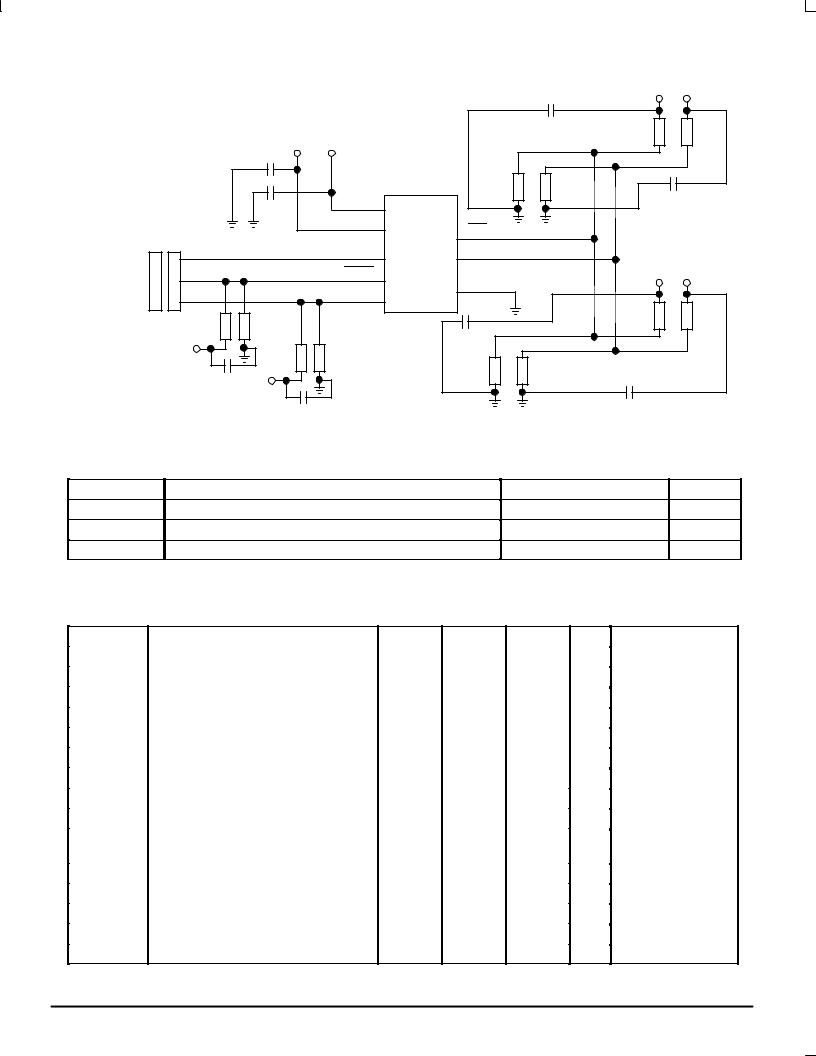
Figure 5. ABSD Interface Design |
|
|
|
||
MAXIMUM RATINGS* |
|
|
|
|
|
|
|
|
|
Symbol |
|
|
Parameter |
|
|
|
Value |
Unit |
|
VCC, VCCO |
DC Supply Voltage (Referenced to GND) |
|
|
|
±0.5 to +7.0 |
V |
|||
TA |
Operating Temperature Range (Ambient) |
|
|
|
0 to +70 |
°C |
|||
TSTG |
Storage Temperature Range |
|
|
|
|
±55 to +125 |
°C |
||
*Maximum Ratings are those values beyond which damage to the device may occur. Functional operation should be restricted to the
Recommended Operating Conditions.
DC CHARACTERISTICS
Symbol |
Characteristic |
|
Min |
Typ |
Max |
Unit |
Condition |
VCC, VCCO |
Supply Voltage |
|
4.75 |
|
5.25 |
V |
|
VIH |
PECL Input High Level |
|
|
|
4.12 |
V |
Note 1. |
VIcut |
PECL Input Cutoff Level |
|
3.00 |
|
3.07 |
V |
Note 1. |
VIL |
PECL Input Low Level |
|
3.19 |
|
|
V |
Note 1. |
VP±PD |
Input Swing Differential |
|
150 |
|
1200 |
mV |
Note 1. |
VP±PC |
Input Swing Start±Up Pulse |
|
300 |
|
1200 |
mV |
Note 1. |
VOH |
PECL Output High Level |
|
3.975 |
|
4.120 |
V |
Note 1. |
VOcut |
PECL Output Cutoff Level |
|
3.00 |
|
3.07 |
V |
Note 1. |
VOL |
PECL Output Low Level |
|
3.19 |
|
3.38 |
V |
Note 1. |
IOUT |
PECL Output Current |
Continuous |
50 |
|
|
mA |
|
|
|
Surge |
100 |
|
|
|
|
|
|
|
|
|
|
|
|
VIHTTL |
Input High TTL |
|
2.0 |
|
|
V |
|
VILTTL |
Input Low TTL |
|
|
|
0.8 |
V |
|
IILTTL |
Input Current Low Level |
|
|
±0.6 |
|
mA |
Vin = 0.5V |
IIHTTL |
Input Current High Level |
|
|
|
|
|
Vin = 2.7V |
CINECL |
Input Capacitance |
|
|
|
2.0 |
pF |
|
1. VCC = 5V; Output Load 25Ω to +3V.
ECLinPS and ECLinPS Lite |
5 |
MOTOROLA |
DL140 Ð Rev 3 |
|
|