Материал: AD620
AD620
Make vs. Buy: A Typical Bridge Application Error Budget
The AD620 offers improved performance over “homebrew” three op amp IA designs, along with smaller size, fewer components and 10¥ lower supply current. In the typical application, shown in Figure 34, a gain of 100 is required to amplify a bridge output of 20 mV full scale over the industrial temperature range of –40°C to +85°C. The error budget table below shows how to calculate the effect various error sources have on circuit accuracy.
Regardless of the system in which it is being used, the AD620 provides greater accuracy, and at low power and price. In simple
systems, absolute accuracy and drift errors are by far the most significant contributors to error. In more complex systems with an intelligent processor, an autogain/autozero cycle will remove all absolute accuracy and drift errors leaving only the resolution errors of gain nonlinearity and noise, thus allowing full 14-bit accuracy.
Note that for the homebrew circuit, the OP07 specifications for input voltage offset and noise have been multiplied by Ö2. This is because a three op amp type in-amp has two op amps at its inputs, both contributing to the overall input error.
|
+10V |
|
|
|
|
|
|
|
|
10kV* |
10kV* |
|
|
|
|
OP07D |
|
R = 350V |
R = 350V |
|
|
|
|
|
|
|
|
10kV** |
|
|
RG |
AD620A |
|
|
|
|
499V |
100V** |
10kV** |
OP07D |
|
R = 350V |
R = 350V |
|
|
|
|
|
|
REFERENCE |
|
|
|
|
|
|
|
OP07D |
|
|
|
|
|
10kV* |
10kV* |
PRECISION BRIDGE TRANSDUCER |
AD620A MONOLITHIC |
“HOMEBREW” IN-AMP, G = 100 |
|
||
INSTRUMENTATION |
|
||||
|
|
AMPLIFIER, G = 100 |
*0.02% RESISTOR MATCH, 3PPM/8C TRACKING |
||
|
|
|
**DISCRETE 1% RESISTOR, 100PPM/8C TRACKING |
||
|
|
|
|
SUPPLY CURRENT = 15mA MAX |
|
|
SUPPLY CURRENT = 1.3mA MAX |
|
|
|
|
Figure 34. Make vs. Buy
Table I. Make vs. Buy Error Budget
|
AD620 Circuit |
“Homebrew” Circuit |
Error, ppm of Full Scale |
||
Error Source |
Calculation |
Calculation |
AD620 |
|
Homebrew |
|
|||||
|
|
|
|
|
|
ABSOLUTE ACCURACY at TA = +25°C |
|
|
|
|
|
Input Offset Voltage, mV |
125 mV/20 mV |
(150 mV ¥ Ö2)/20 mV |
6,250 |
|
10,607 |
Output Offset Voltage, mV |
1000 mV/100/20 mV |
((150 mV ¥ 2)/100)/20 mV |
500 |
|
150 |
Input Offset Current, nA |
2 nA ¥ 350 W/20 mV |
(6 nA ¥ 350 W)/20 mV |
18 |
|
53 |
CMR, dB |
110 dBÆ3.16 ppm, ¥ 5 V/20 mV |
(0.02% Match ¥ 5 V)/20 mV/100 |
791 |
|
500 |
|
|
|
|
|
|
|
|
Total Absolute Error |
7,558 |
|
11,310 |
DRIFT TO +85°C |
|
|
|
|
|
Gain Drift, ppm/°C |
(50 ppm + 10 ppm) ¥ 60°C |
100 ppm/°C Track ¥ 60°C |
3,600 |
|
6,000 |
Input Offset Voltage Drift, mV/°C |
1 mV/°C ¥ 60°C/20 mV |
(2.5 mV/°C ¥ Ö2 ¥ 60°C)/20 mV |
3,000 |
|
10,607 |
Output Offset Voltage Drift, mV/°C |
15 mV/°C ¥ 60°C/100/20 mV |
(2.5 mV/°C ¥ 2 ¥ 60°C)/100/20 mV |
450 |
|
150 |
|
|
|
|
|
|
|
|
Total Drift Error |
7,050 |
|
16,757 |
RESOLUTION |
|
|
|
|
|
Gain Nonlinearity, ppm of Full Scale |
40 ppm |
40 ppm |
40 |
|
40 |
Typ 0.1 Hz–10 Hz Voltage Noise, mV p-p |
0.28 mV p-p/20 mV |
(0.38 mV p-p ¥ Ö2)/20 mV |
14 |
|
27 |
|
|
|
|
|
|
|
|
Total Resolution Error |
54 |
|
67 |
|
|
|
|
|
|
|
|
|
|
|
|
|
|
Grand Total Error |
14,662 |
|
28,134 |
|
|
|
|
|
|
G = 100, VS = ± 15 V. |
|
|
|
|
|
(All errors are min/max and referred to input.) |
|
|
|
|
|
REV. E |
–11– |
AD620
|
+5V |
|
|
|
|
|
|
|
|
|
7 |
20kV |
|
|
|
|
|
3 |
|
|
|
||
3kV |
3kV |
|
|
|
|
||
8 |
|
|
REF |
|
|||
|
|
|
|
|
|||
|
|
|
|
|
|
||
|
|
G=100 |
AD620B |
6 |
IN |
DIGITAL |
|
3kV |
3kV |
499V |
5 |
10kV |
ADC |
||
DATA |
|||||||
|
|
1 |
|||||
|
|
2 |
4 |
|
|
OUTPUT |
|
|
|
|
|
|
|||
|
|
|
|
AD705 |
AGND |
|
|
|
|
|
|
20kV |
|
|
|
1.7mA |
|
|
1.3mA |
0.6mA |
|
|
|
|
|
0.10mA |
|
|
|||
|
|
|
MAX |
MAX |
|
|
|
|
|
|
|
|
|
Figure 35. A Pressure Monitor Circuit which Operates on a +5 V Single Supply
Pressure Measurement
Although useful in many bridge applications such as weigh scales, the AD620 is especially suitable for higher resistance pressure sensors powered at lower voltages where small size and low power become more significant.
Figure 35 shows a 3 kΩ pressure transducer bridge powered from +5 V. In such a circuit, the bridge consumes only 1.7 mA. Adding the AD620 and a buffered voltage divider allows the signal to be conditioned for only 3.8 mA of total supply current.
Small size and low cost make the AD620 especially attractive for voltage output pressure transducers. Since it delivers low noise and drift, it will also serve applications such as diagnostic noninvasive blood pressure measurement.
Medical ECG
The low current noise of the AD620 allows its use in ECG monitors (Figure 36) where high source resistances of 1 MΩ or higher are not uncommon. The AD620’s low power, low supply voltage requirements, and space-saving 8-lead mini-DIP and SOIC package offerings make it an excellent choice for battery powered data recorders.
Furthermore, the low bias currents and low current noise coupled with the low voltage noise of the AD620 improve the dynamic range for better performance.
The value of capacitor C1 is chosen to maintain stability of the right leg drive loop. Proper safeguards, such as isolation, must be added to this circuit to protect the patient from possible harm.
PATIENT/CIRCUIT |
|
|
+3V |
|
|
|
||
|
|
|
|
|
|
|||
PROTECTION/ISOLATION |
|
|
|
|
|
|
||
|
R1 |
R3 |
|
|
0.03Hz |
|
|
|
C1 |
10kV |
24.9kV |
RG |
|
|
|
||
AD620A |
HIGH |
G = 143 |
OUTPUT |
|||||
|
|
|
||||||
|
|
R2 |
8.25kV |
|
PASS |
|
1V/mV |
|
|
R4 |
|
G = 7 |
FILTER |
|
|
||
|
1MV |
24.9kV |
|
|
|
|
|
|
|
|
|
|
|
|
OUTPUT |
|
|
|
|
|
|
|
|
AMPLIFIER |
|
|
AD705J |
|
|
|
|
|
|
||
|
|
|
|
–3V |
|
|
|
|
Figure 36. A Medical ECG Monitor Circuit
–12– |
REV. E |
AD620
Precision V-I Converter
The AD620, along with another op amp and two resistors, makes a precision current source (Figure 37). The op amp buffers the reference terminal to maintain good CMR. The output voltage VX of the AD620 appears across R1, which converts it to a current. This current less only, the input bias current of the op amp, then flows out to the load.
|
|
|
+VS |
|
|
|
VIN+ |
|
3 |
|
7 |
|
|
|
|
8 |
|
|
|
+ VX – |
|
RG |
|
AD620 |
|||
|
|
6 |
||||
|
|
1 |
|
|
5 |
R1 |
|
|
|
|
|
||
VIN– |
|
2 |
|
4 |
|
IL |
|
|
|
|
|
|
|
|
|
|
–V |
|
||
|
|
|
|
S |
AD705 |
|
|
|
|
|
|
|
|
|
I = Vx |
[(V |
IN+ |
) – (V |
)] G |
|
|
= |
IN– |
|
|||
|
L |
R1 |
|
|
R1 |
LOAD |
|
|
|
|
|||
|
|
|
|
|
|
|
Figure 37. Precision Voltage-to-Current Converter (Operates on 1.8 mA, ±3 V)
GAIN SELECTION
The AD620’s gain is resistor programmed by RG, or more precisely, by whatever impedance appears between Pins 1 and 8. The AD620 is designed to offer accurate gains using 0.1%–1% resistors. Table II shows required values of RG for various gains. Note that for G = 1, the RG pins are unconnected (RG = ¥). For any arbitrary gain RG can be calculated by using the formula:
= 49.4 kW
RG G - 1
To minimize gain error, avoid high parasitic resistance in series with RG; to minimize gain drift, RG should have a low TC—less than 10 ppm/°C—for the best performance.
Table II. Required Values of Gain Resistors
1% Std Table |
Calculated |
0.1% Std Table |
Calculated |
Value of RG, V |
Gain |
Value of RG, V |
Gain |
49.9 k |
1.990 |
49.3 k |
2.002 |
12.4 k |
4.984 |
12.4 k |
4.984 |
5.49 k |
9.998 |
5.49 k |
9.998 |
|
|
|
|
2.61 k |
19.93 |
2.61 k |
19.93 |
1.00 k |
50.40 |
1.01 k |
49.91 |
499 |
100.0 |
499 |
100.0 |
|
|
|
|
249 |
199.4 |
249 |
199.4 |
100 |
495.0 |
98.8 |
501.0 |
49.9 |
991.0 |
49.3 |
1,003 |
|
|
|
|
INPUT AND OUTPUT OFFSET VOLTAGE
The low errors of the AD620 are attributed to two sources, input and output errors. The output error is divided by G when referred to the input. In practice, the input errors dominate at high gains and the output errors dominate at low gains. The total VOS for a given gain is calculated as:
Total Error RTI = input error + (output error/G) Total Error RTO = (input error ¥ G) + output error
REFERENCE TERMINAL
The reference terminal potential defines the zero output voltage, and is especially useful when the load does not share a precise ground with the rest of the system. It provides a direct means of injecting a precise offset to the output, with an allowable range of 2 V within the supply voltages. Parasitic resistance should be kept to a minimum for optimum CMR.
INPUT PROTECTION
The AD620 features 400 W of series thin film resistance at its inputs, and will safely withstand input overloads of up to ±15 V or ±60 mA for several hours. This is true for all gains, and power on and off, which is particularly important since the signal source and amplifier may be powered separately. For longer time periods, the current should not exceed 6 mA (IIN £ VIN/400 W). For input overloads beyond the supplies, clamping the inputs to the supplies (using a low leakage diode such as an FD333) will reduce the required resistance, yielding lower noise.
RF INTERFERENCE
All instrumentation amplifiers can rectify out of band signals, and when amplifying small signals, these rectified voltages act as small dc offset errors. The AD620 allows direct access to the input transistor bases and emitters enabling the user to apply some first order filtering to unwanted RF signals (Figure 38), where RC < 1/(2 pf) and where f ³ the bandwidth of the AD620; C £ 150 pF. Matching the extraneous capacitance at Pins 1 and 8 and Pins 2 and 3 helps to maintain high CMR.
|
|
RG |
|
1 |
8 |
|
C |
|
|
R |
|
–IN |
2 |
7 |
+IN |
R |
|
3 |
6 |
|
|
4 |
5 |
|
C |
|
Figure 38. Circuit to Attenuate RF Interference
REV. E |
–13– |
AD620
COMMON-MODE REJECTION
Instrumentation amplifiers like the AD620 offer high CMR, which is a measure of the change in output voltage when both inputs are changed by equal amounts. These specifications are usually given for a full-range input voltage change and a specified source imbalance.
For optimal CMR the reference terminal should be tied to a low impedance point, and differences in capacitance and resistance should be kept to a minimum between the two inputs. In many applications shielded cables are used to minimize noise, and for best CMR over frequency the shield should be properly driven. Figures 39 and 40 show active data guards that are configured to improve ac common-mode rejections by “bootstrapping” the capacitances of input cable shields, thus minimizing the capacitance mismatch between the inputs.
+VS
– INPUT
AD648
100V
|
RG |
AD620 |
VOUT |
100V |
–V |
|
|
|
S |
|
|
|
|
|
REFERENCE |
+ INPUT
–V
S
Figure 39. Differential Shield Driver
|
|
+VS |
|
– INPUT |
|
|
|
|
RG |
|
|
100V |
2 |
AD620 |
VOUT |
AD548 |
RG |
||
|
|
|
|
|
2 |
|
|
|
|
|
REFERENCE |
+ INPUT |
|
|
|
|
|
–V |
|
|
|
S |
|
Figure 40. Common-Mode Shield Driver
GROUNDING
Since the AD620 output voltage is developed with respect to the potential on the reference terminal, it can solve many grounding problems by simply tying the REF pin to the appropriate “local ground.”
In order to isolate low level analog signals from a noisy digital environment, many data-acquisition components have separate analog and digital ground pins (Figure 41). It would be convenient to use a single ground line; however, current through ground wires and PC runs of the circuit card can cause hundreds of millivolts of error. Therefore, separate ground returns should be provided to minimize the current flow from the sensitive points to the system ground. These ground returns must be tied together at some point, usually best at the ADC package as shown.
ANALOG P.S. |
|
DIGITAL P.S. |
+15V C –15V |
|
C +5V |
0.1mF |
0.1mF |
|
|
|
1mF |
1mF |
1mF |
|
|
|
+ |
AD620 |
AD585 |
AD574A |
DIGITAL |
|
DATA |
||
|
S/H |
ADC |
|
|
OUTPUT |
||
|
|
|
Figure 41. Basic Grounding Practice
–14– |
REV. E |
AD620
GROUND RETURNS FOR INPUT BIAS CURRENTS
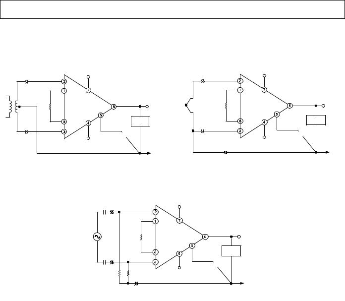
Input bias currents are those currents necessary to bias the input transistors of an amplifier. There must be a direct return path for these currents; therefore, when amplifying “floating” input
|
+VS |
|
– INPUT |
|
|
RG |
AD620 |
VOUT |
|
|
LOAD |
+ INPUT |
|
REFERENCE |
|
–V |
|
|
S |
|
|
|
TO POWER |
|
|
SUPPLY |
|
|
GROUND |
Figure 42a. Ground Returns for Bias Currents with Transformer Coupled Inputs
sources such as transformers, or ac-coupled sources, there must be a dc path from each input to ground as shown in Figure 42. Refer to the Instrumentation Amplifier Application Guide (free from Analog Devices) for more information regarding in amp applications.
+VS
– INPUT
RG |
AD620 |
VOUT |
|
|
LOAD |
+ INPUT |
|
REFERENCE |
|
–V |
|
|
S |
|
|
|
TO POWER |
|
|
SUPPLY |
|
|
GROUND |
Figure 42b. Ground Returns for Bias Currents with Thermocouple Inputs
|
|
+VS |
|
|
– INPUT |
|
|
|
RG |
AD620 |
VOUT |
|
|
|
LOAD |
|
+ INPUT |
|
REFERENCE |
100kV |
100kV |
–V |
|
S |
|
||
|
|
|
TO POWER |
|
|
|
SUPPLY |
|
|
|
GROUND |
Figure 42c. Ground Returns for Bias Currents with AC Coupled Inputs
REV. E |
–15– |