Материал: sn74ahct1g08
SN74AHCT1G08
SCLS315Q –MARCH 1996 –REVISED APRIL 2016 |
|
|
|
|
|
|
|
|
|
|
|
|
|
|
|
|
|
|
|
|
www.ti.com |
|||||||||||||||||
7 Parameter Measurement Information |
|
|
|
|
|
|
|
|
|
|
|
|
|
|
|
|
|
|
|
|
|
|
||||||||||||||||
|
|
|
|
|
|
|
|
|
|
|
|
|
|
|
|
|
|
|
|
|
VCC |
|
|
|
|
|
|
|
|
|
|
|
||||||
|
|
|
|
|
|
|
|
|
|
|
|
|
|
|
|
|
|
|
Ω S1 |
|
|
|
|
|
|
|
|
|
|
|
|
|||||||
|
|
|
|
|
|
|
|
|
|
|
|
|
|
|
|
|
RL = 1 |
Open |
|
|
TEST |
|
|
S1 |
|
|||||||||||||
From Output |
|
|
|
|
|
Test |
From Output |
|
k |
|
|
|
|
|
|
|
|
|
|
|
|
|||||||||||||||||
|
|
|
|
GND |
|
|
|
|
|
|
|
|||||||||||||||||||||||||||
Under Test |
|
|
|
|
Point |
Under Test |
|
|
|
|
|
tPLH/tPHL |
|
|
Open |
|
||||||||||||||||||||||
|
|
|
|
|
|
|
|
|
|
|
|
|
|
|
|
|
|
|
||||||||||||||||||||
CL |
|
|
|
|
|
|
|
|
|
|
CL |
|
|
|
|
|
|
|
|
|
|
|
|
|
tPLZ/tPZL |
|
|
VCC |
|
|||||||||
(see Note A) |
|
|
|
|
|
|
|
|
|
(see Note A) |
|
|
|
|
|
|
|
|
|
|
|
|
|
tPHZ/tPZH |
|
|
GND |
|
||||||||||
|
|
|
|
|
|
|
|
|
|
|
|
|
|
|
|
|
|
|
|
|
|
|
|
|
|
|
|
|
|
|
|
|||||||
|
|
|
|
|
|
|
|
|
|
|
|
|
|
|
|
|
|
|
|
|
|
|
|
|
|
|
|
|
Open Drain |
|
|
VCC |
|
|||||
LOAD CIRCUIT FOR |
|
|
|
|
LOAD CIRCUIT FOR |
|
|
|
|
|
|
|
|
|
|
|
|
|
|
|
|
|
|
|||||||||||||||
TOTEM-POLE OUTPUTS |
|
|
|
3-STATE AND OPEN-DRAIN OUTPUTS |
|
|
|
|
|
|
|
|
|
|
|
|
|
|
|
|
|
|
||||||||||||||||
|
|
|
|
|
|
|
|
|
|
|
|
|
|
|
|
|
|
|
|
|
|
|
|
|
|
|
|
|
|
|
|
|
|
|
|
|
3 V |
|
|
|
|
|
|
|
|
|
|
|
|
|
|
|
|
|
|
|
Timing Input |
|
|
|
|
|
|
|
|
1.5 V |
|
|
0 V |
||||||||
|
|
|
|
|
|
|
|
|
|
|
|
|
|
|
|
|
|
|
|
|
|
|
|
|
|
|
||||||||||||
|
|
|
|
|
|
|
|
|
|
|
|
|
|
|
|
|
|
|
|
|
|
|
|
|
|
|
|
|
|
|
|
|
|
|
|
|
||
|
|
|
|
|
|
|
|
|
|
tw |
|
|
|
|
|
|
|
|
|
|
|
|
|
|
|
|
|
|
|
|
|
|
|
|
|
|
||
|
|
|
|
|
|
|
|
|
|
|
|
|
|
|
|
|
|
|
|
|
|
|
|
|
|
|
|
|
|
|
|
|
|
|
|
|
|
|
|
|
|
|
|
|
|
|
|
|
|
|
|
|
|
|
|
|
|
|
|
|
|
|
|
|
|
|
|
|
|
|
|
th |
|
|
|
|
|
|
|
|
|
|
|
|
|
|
|
|
|
|
|
|
|
|
|
|
|
|
|
|
|
|
|
|
|
|
|
|
|
|
|
|
|
|
|
|
|
|
|
|
|
|
|
|
|
|
|
|
|
|
|
|
|
|
|
|
|
|
|
|
|
|
|
|
|
|
|
|
|
|
|
|
|
||
|
|
|
|
|
|
|
|
|
|
|
|
|
|
|
3 V |
|
|
|
|
tsu |
|
|
|
|
|
|
|
|
|
|
|
|
|
|
|
3 V |
||
|
|
|
|
|
|
|
|
|
|
|
|
|
|
|
|
|
|
|
|
|
|
|
|
|
|
|
|
|
||||||||||
|
|
|
|
|
1.5 V |
|
|
|
1.5 V |
|
|
|
|
|
|
|
|
|
|
|
|
|
|
|
|
|
|
|
|
|||||||||
|
|
|
|
|
|
|
|
|
|
|
|
|
|
|
|
|
|
|
|
|
|
|
|
|
|
|
|
|
|
|||||||||
Input |
|
|
|
|
|
|
Data Input |
|
|
|
|
1.5 V |
|
|
|
|
1.5 V |
|
|
|
|
|||||||||||||||||
|
|
|
|
|
|
|
|
|
|
|
|
|
|
|
0 V |
|
|
|
|
|
|
|
|
|
|
|
|
0 V |
||||||||||
|
|
|
|
|
|
|
|
|
|
|
|
|
|
|
|
|
|
|
|
|
|
|
|
|
|
|
|
|
|
|
|
|
||||||
|
|
|
|
|
|
|
|
|
|
|
|
|
|
|
|
|
|
|
|
|
|
|
|
|
|
|
|
|
|
|
|
|
|
|
||||
VOLTAGE WAVEFORMS
PULSE DURATION
|
|
|
3 V |
Input |
1.5 V |
1.5 V |
|
|
|
|
0 V |
|
tPLH |
|
tPHL |
In-Phase |
|
|
VOH |
|
50% VCC |
50% VCC |
|
Output |
|
||
|
|
VOL |
|
|
|
|
|
|
tPHL |
|
tPLH |
Out-of-Phase |
|
|
VOH |
|
50% VCC |
50% VCC |
|
|
|
Output
VOL
VOLTAGE WAVEFORMS
PROPAGATION DELAY TIMES
INVERTING AND NONINVERTING OUTPUTS
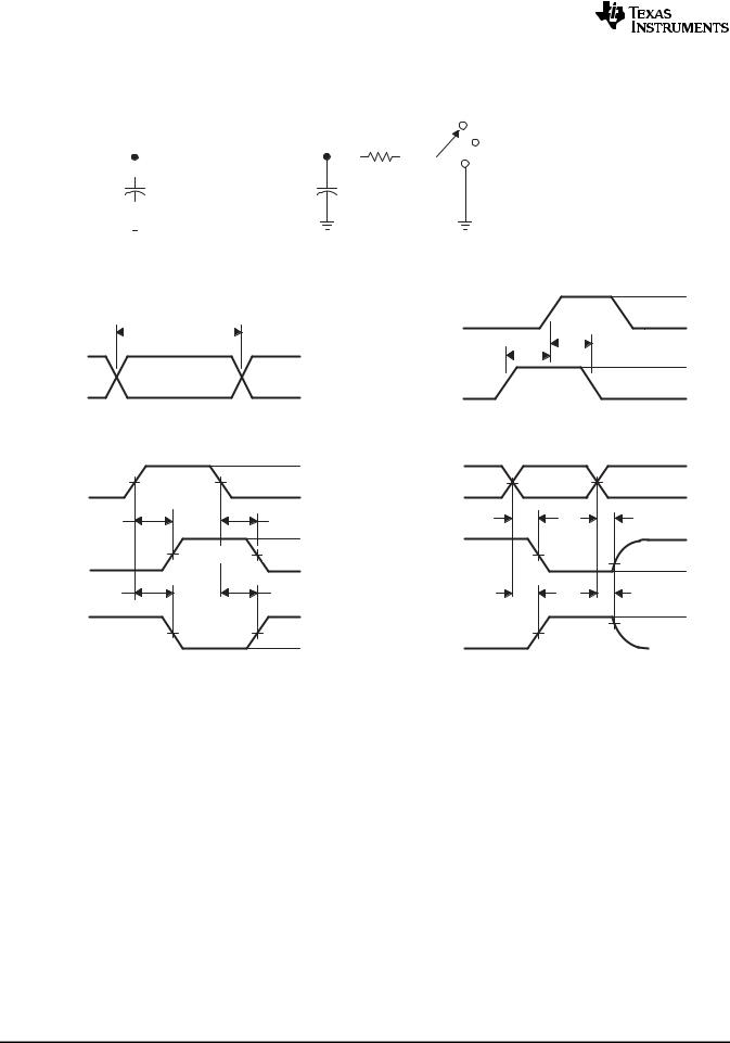
CL includes probe and jig capacitance.
VOLTAGE WAVEFORMS
SETUP AND HOLD TIMES
Output |
|
3 V |
|
1.5 V |
1.5 V |
||
Control |
|||
|
0 V |
||
|
|
||
tPZL |
|
tPLZ |
|
Output |
|
≈VCC |
|
Waveform 1 |
50% VCC |
||
S1 at VCC |
VOL + 0.3 V |
||
|
|||
(see Note B) |
|
VOL |
|
tPZH |
|
tPHZ |
|
Output |
|
VOH |
|
Waveform 2 |
|
||
S1 at GND |
50% VCC |
VOH − 0.3 V |
(see Note B) |
|
|
≈0 V |
|
|
||
|
|
|
|
|
VOLTAGE WAVEFORMS |
||
ENABLE AND DISABLE TIMES
LOWAND HIGH-LEVEL ENABLING
Waveform 1 is for an output with internal conditions such that the output is low except when disabled by the output control.
Waveform 2 is for an output with internal conditions such that the output is high except when disabled by the output control.
All input pulses are supplied by generators having the following characteristics: PRR ≤ 1 MHz, ZO = 50 Ω, tr ≤ 3 ns, tf ≤ 3 ns.
The outputs are measured one at a time with one input transition per measurement.
All parameters and waveforms are not applicable to all devices.
Figure 2. Load Circuit and Voltage Waveforms
6 |
Submit Documentation Feedback |
Copyright © 1996–2016, Texas Instruments Incorporated |
Product Folder Links: SN74AHCT1G08

SN74AHCT1G08
www.ti.com |
SCLS315Q –MARCH 1996–REVISED APRIL 2016 |
8 Detailed Description
8.1 Overview
The SN74AHCT1G08 device is a single 2-input positive-AND gate. The device performs the Boolean AND function (Y = A • B or Y = A + B) in positive logic. Low ICC current allows this device to be used in powersensitive or battery-powered applications. Robust inputs allow the device to up-translate with a propagation delay of 20 ns.
8.2 Functional Block Diagram
A |
1 |
|
|
|
|
|
4 |
Y |
|||
2 |
|||||
B |
|
|
|||
|
|
||||
|
|
|
|||
|
|
|
|
||
|
|
|
|
||
Figure 3. Logic Diagram (Positive Logic)
8.3 Feature Description
The VCC for the device is optimized at 5 V.
Up voltage translation from 3.3 V to 5 V is allowed. The inputs accept VIH levels of 2 V. Output ringing is minimized by slow edge rates.
Inputs are TTL-Voltage compatible.
8.4 Device Functional Modes
Table 1 lists the functional modes of the SN74AHCT1G08.
Table 1. Function Table
|
INPUTS |
OUTPUT |
|
A |
|
B |
Y |
H |
|
H |
H |
L |
|
X |
L |
X |
|
L |
L |
Copyright © 1996–2016, Texas Instruments Incorporated |
Submit Documentation Feedback |
7 |
Product Folder Links: SN74AHCT1G08
SN74AHCT1G08
SCLS315Q –MARCH 1996 –REVISED APRIL 2016 |
www.ti.com |
9 Application and Implementation
NOTE
Information in the following applications sections is not part of the TI component specification, and TI does not warrant its accuracy or completeness. TI’s customers are responsible for determining suitability of components for their purposes. Customers should validate and test their design implementation to confirm system functionality.
9.1 Application Information
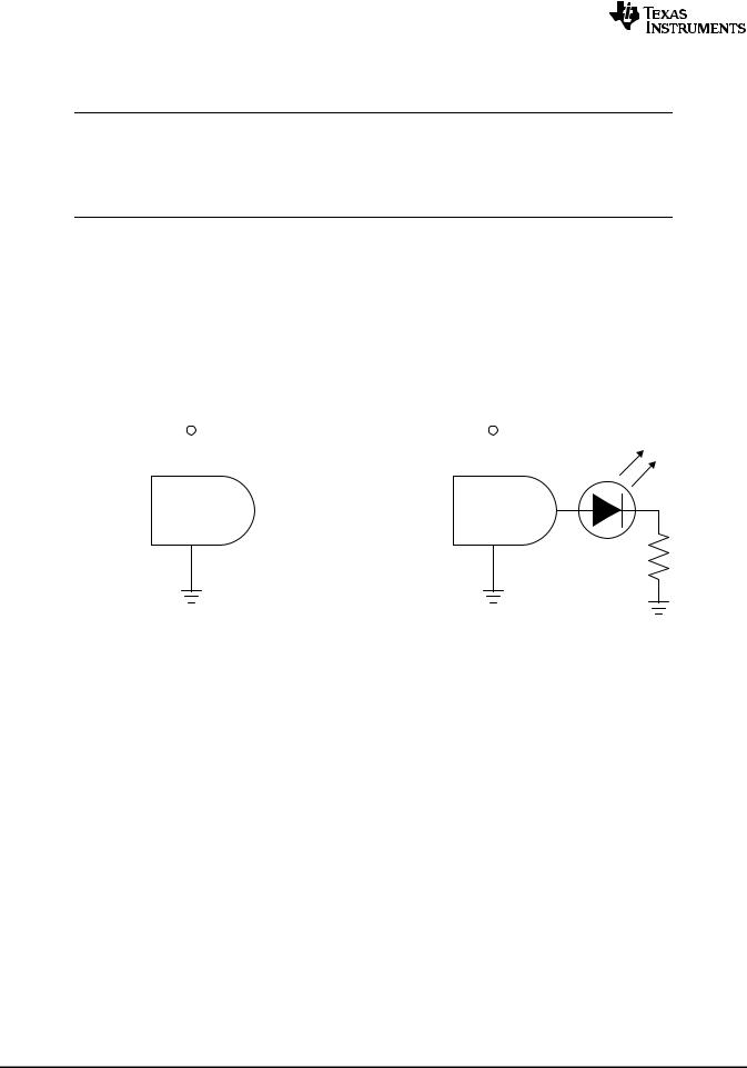
The SN74AHCT1G08 device is a single AND gate, which is often used for many common functions like power sequencing or an on LED indicator. Because the device is configured to output LOW unless all inputs are HIGH, an LED tied to the output of the device will only turn HIGH when all systems connected are sending a HIGH, or ready signal.
9.2 Typical Application
|
|
AND Logic Function |
|
|
|
Basic LED Driver |
|||
|
|
|
VCC |
|
|
|
VCC |
||
A– uC or Logic |
|
|
|
|
A– uC or Logic |
|
|
||
|
|
|
|
|
|
||||
|
|
|
|
|
|
|
|
|
|
|
|
|
|
|
Y– uC or Logic |
|
|
||
B– uC or Logic |
|
AHCT1G08 |
|
B– uC or Logic |
AHCT1G08 |
||||
|
|
||||||||
|
|
|
|
|
|
||||
|
|
|
|
|
|
|
|
|
|
Copyright © 2016, Texas Instruments Incorporated
Figure 4. Typical Application Diagram
9.2.1 Design Requirements
This device uses CMOS technology and has balanced output drive. Take care to avoid bus contention because it can drive currents that would exceed maximum limits. The high drive also creates fast edges into light loads, so routing and load conditions must be considered to prevent ringing.
9.2.2 Detailed Design Procedure
1. Recommended Input Conditions
– For rise time and fall time specifications, see t/ V in Recommended Operating Conditions.
–For specified high and low levels, see VIH and VIL in Recommended Operating Conditions.
–Inputs are overvoltage tolerant allowing them to go as high as 5.5 V at any valid VCC.
2.Recommended Output Conditions
–Load currents must not exceed 25 mA per output and 50 mA total for the part.
–Outputs must not be pulled above VCC.
8 |
Submit Documentation Feedback |
Copyright © 1996–2016, Texas Instruments Incorporated |
Product Folder Links: SN74AHCT1G08
SN74AHCT1G08
www.ti.com |
SCLS315Q –MARCH 1996–REVISED APRIL 2016 |
Typical Application (continued)
9.2.3 Application Curve
Voltage (V)
5.5 |
|
|
|
|
|
|
|
|
|
|
5 |
|
|
|
|
|
|
|
|
AHCT1G08 |
|
|
|
|
|
|
|
|
|
AC |
|
|
|
|
|
|
|
|
|
|
|
|
|
4.5 |
|
|
|
|
|
|
|
|
HC |
|
4 |
|
|
|
|
|
|
|
|
VI |
|
|
|
|
|
|
|
|
|
|
|
|
3.5 |
|
|
|
|
|
|
|
|
|
|
3 |
|
|
|
|
|
|
|
|
|
|
2.5 |
|
|
|
|
|
|
|
|
|
|
2 |
|
|
|
|
|
|
|
|
|
|
1.5 |
|
|
|
|
|
|
|
|
|
|
1 |
|
|
|
|
|
|
|
|
|
|
0.5 |
|
|
|
|
|
|
|
|
|
|
0 |
|
|
|
|
|
|
|
|
|
|
–0.5 |
|
|
|
|
|
|
|
|
|
|
–1.5 |
|
|
|
|
|
|
|
|
|
|
0 |
2 |
4 |
6 |
8 |
10 |
12 |
14 |
16 |
18 |
20 |
|
|
|
|
|
Time (ns) |
|
|
|
|
|
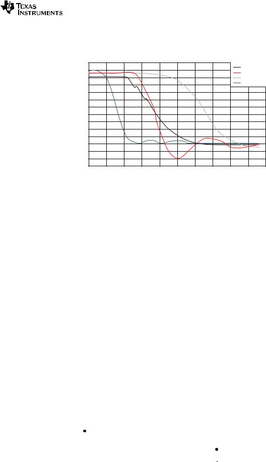
VCC = 5 V |
Load = 50 Ω / 50 pF |
Figure 5. Typical Switching Characteristics
10 Power Supply Recommendations
The power supply can be any voltage between the minimum and maximum supply voltage rating located in
Recommended Operating Conditions.
Each VCC pin must have a good bypass capacitor to prevent power disturbance. TI recommends a 0.1-µF capacitor for devices with a single supply; and a 0.01-µF or 0.022-µF capactor for each power pin if there are multiple VCC pins. It is ok to parallel multiple bypass capacitors to reject different frequencies of noise. 0.1-μF and 1-μF capacitors are commonly used in parallel. The bypass capacitor must be installed as close to the power pin as possible for best results.
11 Layout
11.1 Layout Guidelines
When using multiple bit logic devices inputs must not ever float. In many cases, functions or parts of functions of digital logic devices are unused; for example, when only two inputs of a triple-input AND gate are used or only 3 of the 4 buffer gates are used. Such input pins must not be left unconnected because the undefined voltages at the outside connections result in undefined operational states. Observe the following rules under all circumstances.
•All unused inputs of digital logic devices must be connected to a high or low bias to prevent them from floating.
•The logic level that must be applied to any particular unused input depends on the function of the device. Generally they will be tied to GND or VCC, whichever make more sense or is more convenient.
11.2 Layout Example
VCC |
|
|
|
|
|
Input |
|
|
|
|
|
|
|
|
|
|
|
|
|
|
|
|
|
|
|
|
|
|
|
||
Unused Input |
|
|
|
Output |
Unused Input |
|
|
|
|
|
Output |
||||
Input |
|
|
|
|
|
|
|
|
|
|
|
|
|
|
|
|
|
|
|
|
|
|
|
|
|
|
|
|
|
||
|
|
|
|
|
|
|
|
|
|
|
|
|
|
|
|
|
|
|
|
|
|
|
|
|
|
|
|
|
|
|
|
|
|
|
|
|
|
|
|
|
|
|
|
|
|
|
|
Figure 6. |
Layout Diagram |
|
|
|
|
Copyright © 1996–2016, Texas Instruments Incorporated |
Submit Documentation Feedback |
9 |
Product Folder Links: SN74AHCT1G08

SN74AHCT1G08
SCLS315Q –MARCH 1996 –REVISED APRIL 2016 |
www.ti.com |
12 Device and Documentation Support
12.1 Documentation Support
12.1.1 Related Documentation
For related documentation, see the following:
Implications of Slow or Floating CMOS Inputs, SCBA004
12.2 Community Resources
The following links connect to TI community resources. Linked contents are provided "AS IS" by the respective contributors. They do not constitute TI specifications and do not necessarily reflect TI's views; see TI's Terms of Use.
TI E2E™ Online Community TI's Engineer-to-Engineer (E2E) Community. Created to foster collaboration among engineers. At e2e.ti.com, you can ask questions, share knowledge, explore ideas and help solve problems with fellow engineers.
Design Support TI's Design Support Quickly find helpful E2E forums along with design support tools and contact information for technical support.
12.3 Trademarks
E2E is a trademark of Texas Instruments.
All other trademarks are the property of their respective owners.
12.4 Electrostatic Discharge Caution
This integrated circuit can be damaged by ESD. Texas Instruments recommends that all integrated circuits be handled with appropriate precautions. Failure to observe proper handling and installation procedures can cause damage.
ESD damage can range from subtle performance degradation to complete device failure. Precision integrated circuits may be more susceptible to damage because very small parametric changes could cause the device not to meet its published specifications.
12.5 Glossary
SLYZ022 — TI Glossary.
This glossary lists and explains terms, acronyms, and definitions.
13 Mechanical, Packaging, and Orderable Information
The following pages include mechanical packaging and orderable information. This information is the most current data available for the designated devices. This data is subject to change without notice and revision of this document. For browser based versions of this data sheet, refer to the left hand navigation.
10 |
Submit Documentation Feedback |
Copyright © 1996–2016, Texas Instruments Incorporated |
Product Folder Links: SN74AHCT1G08