Материал: tvs2
Transient Voltage Suppressors Ð Surface Mounted
24 Watt Peak Power
|
A |
|
|
L |
|
|
3 |
S |
|
B |
|
1 |
2 |
|
V |
G |
|
|
|
C |
|
D |
H |
K |
J |
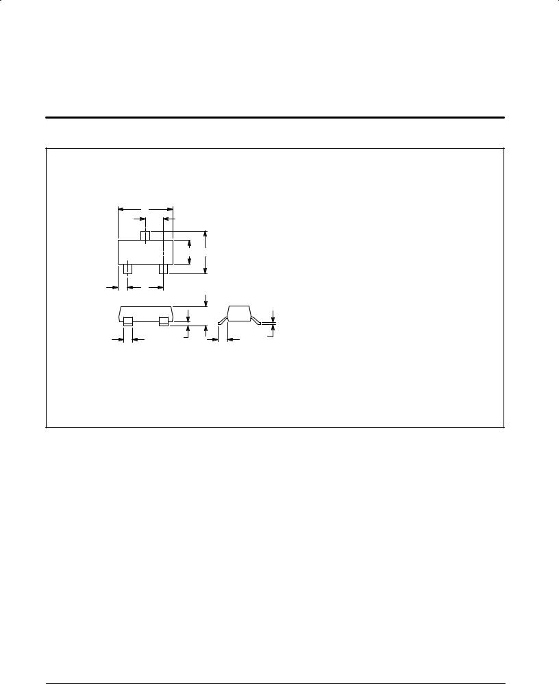
NOTES:
1.DIMENSIONING AND TOLERANCING PER ANSI Y14.5M, 1982.
2.CONTROLLING DIMENSION: INCH.
3.MAXIMUM LEAD THICKNESS INCLUDES LEAD FINISH THICKNESS. MINIMUM LEAD THICKNESS IS THE MINIMUM THICKNESS OF BASE MATERIAL.
|
INCHES |
MILLIMETERS |
||
DIM |
MIN |
MAX |
MIN |
MAX |
A |
0.1102 |
0.1197 |
2.80 |
3.04 |
B |
0.0472 |
0.0551 |
1.20 |
1.40 |
C |
0.0350 |
0.0440 |
0.89 |
1.11 |
D |
0.0150 |
0.0200 |
0.37 |
0.50 |
G |
0.0701 |
0.0807 |
1.78 |
2.04 |
H |
0.0005 |
0.0040 |
0.013 |
0.100 |
J |
0.0034 |
0.0070 |
0.085 |
0.177 |
K |
0.0180 |
0.0236 |
0.45 |
0.60 |
L |
0.0350 |
0.0401 |
0.89 |
1.02 |
S |
0.0830 |
0.0984 |
2.10 |
2.50 |
V |
0.0177 |
0.0236 |
0.45 |
0.60 |
STYLE 12:
PIN 1. CATHODE
2.CATHODE
3.ANODE
CASE 318-07
PLASTIC
(Refer to Section 10 for Surface Mount, Thermal Data and Footprint Information.)
MULTIPLE PACKAGE QUANTITY (MPQ)
REQUIREMENTS
Package Option |
Type No. Suffix |
MPQ (Units) |
|
|
|
Tape and Reel |
T1 |
3K |
|
|
|
Tape and Reel |
T3 |
10K |
|
|
|
(Refer to Section 10 for more information on Packaging Specifications.)
24 Watt Peak Power Data Sheet |
Motorola TVS/Zener Device Data |
5-60 |
|
MOTOROLA
SEMICONDUCTOR TECHNICAL DATA
Order this document by MMBZ15VDLT1/D
15 & 27 Volt SOT-23 Dual Monolithic Common
Cathode Zeners
Transient Voltage Suppressors for ESD Protection
These dual monolithic silicon zener diodes are designed for applications requiring transient overvoltage protection capability. They are intended for use in voltage and ESD sensitive equipment such as computers, printers, business machines, communication systems, medical equipment and other applications. Their dual junction common cathode design protects two separate lines using only one package. These devices are ideal for situations where board space is at a premium.
Specification Features:
•SOT±23 Package Allows Either Two Separate Unidirectional Configurations or a Single Bidirectional Configuration
•Peak Power Ð 40 Watts @ 1.0 ms (Bidirectional), per Figure 5 Waveform
•Maximum Clamping Voltage @ Peak Pulse Current
•Low Leakage < 100 nA
•ESD Rating of Class N (exceeding 16 kV) per the Human Body Model
Mechanical Characteristics:
•Void Free, Transfer±Molded, Thermosetting Plastic Case
•Corrosion Resistant Finish, Easily Solderable
•Package Designed for Optimal Automated Board Assembly
•Small Package Size for High Density Applications
•Available in 8 mm Tape and Reel
Use the Device Number to order the 7 inch/3,000 unit reel. Replace
the ªT1º with ªT3º in the Device Number to order the 13 inch/10,000 unit reel.
MMBZ15VDLT1
MMBZ27VCLT1
Motorola Preferred Devices
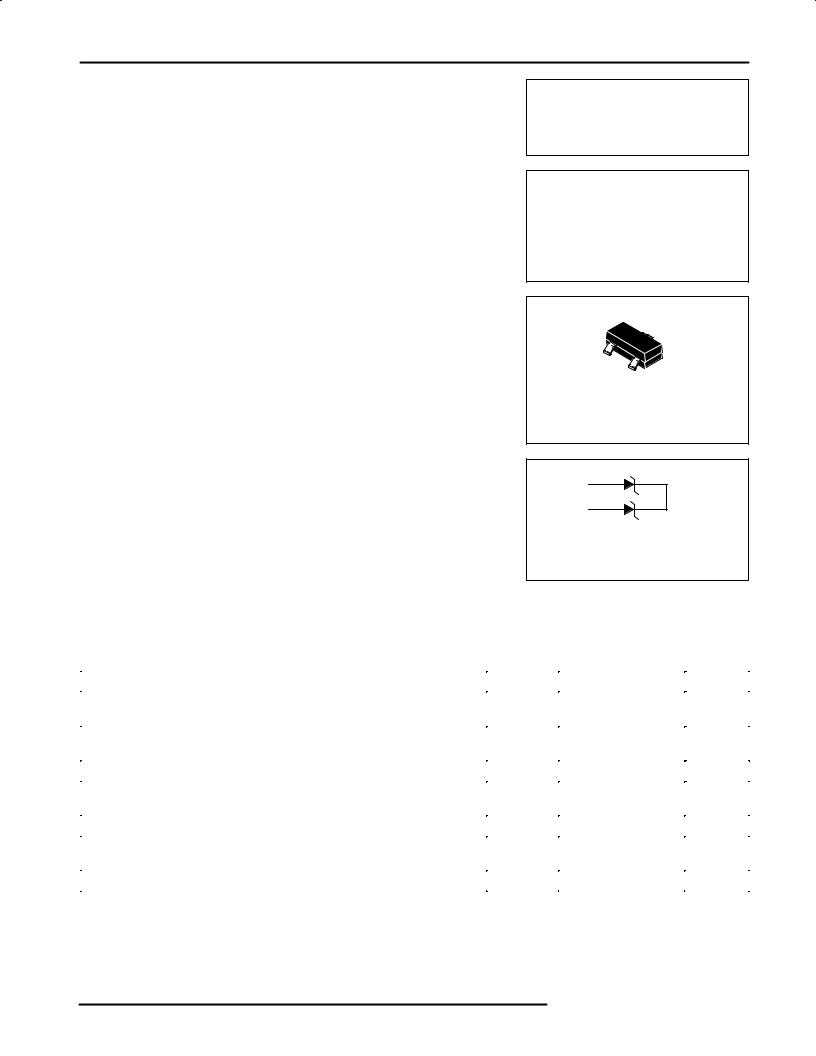
SOT±23
COMMON CATHODE
DUAL ZENER
OVERVOLTAGE
TRANSIENT SUPPRESSORS
40 WATTS
PEAK POWER
3
1
2
CASE 318±08
TO±236AB
LOW PROFILE SOT±23
1 

 3
3
2 
TERMINAL 1 ± ANODE
TERMINAL 2 ± ANODE
TERMINAL 3 ± CATHODE
THERMAL CHARACTERISTICS (TA = 25°C unless otherwise noted)
Characteristic |
Symbol |
Value |
Unit |
|
|
|
|
Peak Power Dissipation @ 1.0 ms (1) |
Ppk |
40 |
Watts |
@ TA ≤ 25°C |
|
|
|
Total Power Dissipation on FR±5 Board (2) @ TA = 25°C |
PD |
225 |
mW |
Derate above 25°C |
|
1.8 |
mW/°C |
|
|
|
|
Thermal Resistance Junction to Ambient |
RθJA |
556 |
°C/W |
Total Power Dissipation on Alumina Substrate (3) @ TA = 25°C |
PD |
300 |
mW |
Derate above 25°C |
|
2.4 |
mW/°C |
|
|
|
|
Thermal Resistance Junction to Ambient |
RθJA |
417 |
°C/W |
Junction and Storage Temperature Range |
TJ |
± 55 to +150 |
°C |
|
Tstg |
|
|
Lead Solder Temperature Ð Maximum (10 Second Duration) |
TL |
230 |
°C |
1.Non±repetitive current pulse per Figure 5 and derate above TA = 25°C per Figure 6.
2.FR±5 = 1.0 x 0.75 x 0.62 in.
3.Alumina = 0.4 x 0.3 x 0.024 in., 99.5% alumina
Thermal Clad is a trademark of the Bergquist Company
Preferred devices are Motorola recommended choices for future use and best overall value.
Rev 1
Motorola, Inc. 1996
MMBZ15VDLT1 MMBZ27VCLT1
61
ELECTRICAL CHARACTERISTICS (TA = 25°C unless otherwise noted)
UNIDIRECTIONAL (Circuit tied to Pins 1 and 3 or Pins 2 and 3)
(VF = 0.9 V Max @ IF = 10 mA)
|
Breakdown Voltage |
|
Reverse Voltage |
Max Reverse |
Max Reverse |
Max Reverse |
Maximum |
|||||
|
|
|
|
|
|
Voltage @ IRSM(5) |
Temperature |
|||||
|
|
VBR(4) |
|
|
|
Working Peak |
Leakage Current |
Surge Current |
||||
|
|
|
|
@ IT |
(Clamping Voltage) |
Coefficient of |
||||||
|
|
(V) |
|
|
V |
RWM |
I |
I |
(5) |
|||
|
|
|
|
|
(mA) |
|
RWM |
|
RSM |
VRSM |
VBR |
|
|
|
|
|
|
|
(V) |
IR (nA) |
|
(A) |
|||
Min |
|
Nom |
Max |
|
|
|
|
(V) |
(mV/°C) |
|||
|
|
|
|
|
|
|
|
|||||
|
|
|
|
|
|
|
|
|
|
|
|
|
14.3 |
|
15 |
15.8 |
|
1.0 |
12.8 |
100 |
|
1.9 |
21.2 |
12 |
|
|
|
|
|
|
|
|
|
|
|
|
|
|
(VF = 1.1 V Max @ IF = 200 mA)
|
Breakdown Voltage |
|
Reverse Voltage |
Max Reverse |
Max Reverse |
Max Reverse |
Maximum |
|||||
|
|
|
|
|
|
Voltage @ IRSM(5) |
Temperature |
|||||
|
|
VBR(4) |
|
|
|
Working Peak |
Leakage Current |
Surge Current |
||||
|
|
|
|
@ IT |
(Clamping Voltage) |
Coefficient of |
||||||
|
|
(V) |
|
|
V |
RWM |
I |
I |
(5) |
|||
|
|
|
|
|
(mA) |
|
RWM |
|
RSM |
VRSM |
VBR |
|
|
|
|
|
|
|
(V) |
IR (nA) |
|
(A) |
|||
Min |
|
Nom |
Max |
|
|
|
|
(V) |
(mV/°C) |
|||
|
|
|
|
|
|
|
|
|||||
|
|
|
|
|
|
|
|
|
|
|
|
|
25.65 |
|
27 |
28.35 |
|
1.0 |
|
22 |
50 |
|
1.0 |
38 |
26 |
|
|
|
|
|
|
|
|
|
|
|
|
|
(4)VBR measured at pulse test current IT at an ambient temperature of 25°C.
(5)Surge current waveform per Figure 5 and derate per Figure 6.
TYPICAL CHARACTERISTICS
|
|
MMBZ15VDLT1 |
|
|
|
17 |
|
|
|
(VOLTS) |
16 |
|
BIDIRECTIONAL |
|
|
|
|
||
|
|
|
|
|
VOLTAGE |
) |
|
|
|
T |
|
|
|
|
@I |
|
|
|
|
15 |
|
|
|
|
BR |
|
|
|
|
BREAKDOWN |
14 |
|
|
|
(V |
|
UNIDIRECTIONAL |
|
|
|
|
|
|
|
|
13 |
|
|
+ 125 |
|
± 40 |
+ 25 |
+ 85 |
|
TEMPERATURE (°C)
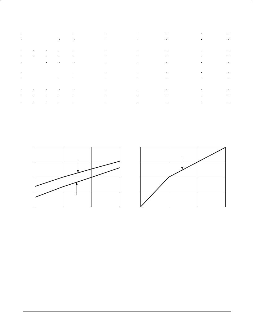
Figure 1A. Typical Breakdown Voltage
versus Temperature
|
|
MMBZ27VCLT1 |
|
|
|
29 |
|
|
|
(VOLTS) |
|
|
BIDIRECTIONAL |
|
28 |
|
|
|
|
|
|
|
|
|
VOLTAGE |
) |
|
|
|
T |
|
|
|
|
@I |
|
|
|
|
27 |
|
|
|
|
BR |
|
|
|
|
BREAKDOWN |
26 |
|
|
|
(V |
|
|
|
|
|
25 |
|
|
+ 125 |
|
± 55 |
+ 25 |
+ 85 |
|
TEMPERATURE (°C)
Figure 1B. Typical Breakdown Voltage
versus Temperature
MOTOROLA |
MMBZ15VDLT1 MMBZ27VCLT1 |
62
10000 |
|
|
|
100 |
|
|
|
10 |
|
|
|
(nA) |
|
|
|
R |
|
|
|
I |
|
|
|
1 |
|
|
|
0.1 |
|
|
|
0.01 |
|
|
|
± 40 |
+ 25 |
+ 85 |
+ 125 |
TEMPERATURE (°C)
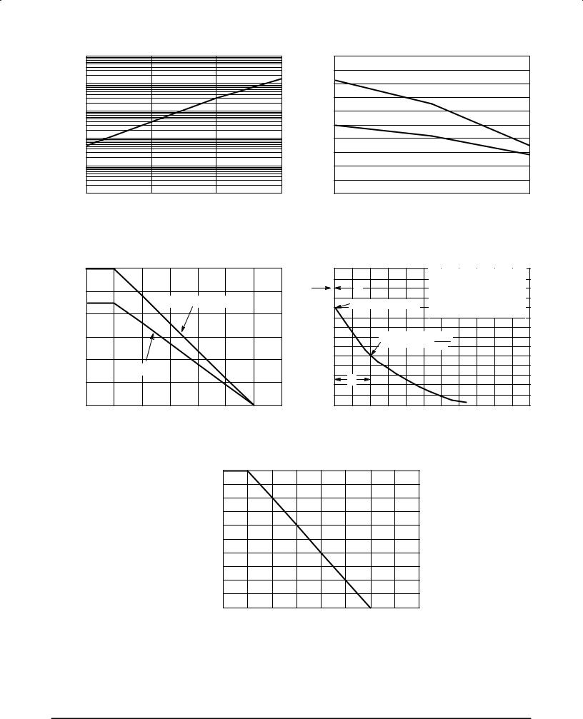
Figure 2. Typical Leakage Current
versus Temperature
|
MMBZ15VDLT1 |
|
|
100 |
|
|
90 |
|
|
80 |
|
(pF) |
70 |
|
UNIDIRECTIONAL |
|
|
CAPACITANCE |
|
|
60 |
|
|
50 |
|
|
40 |
|
|
BIDIRECTIONAL |
|
|
C, |
30 |
|
|
20 |
|
|
10 |
|
|
0 |
12.8 |
|
1 |
BIAS (V)
Figure 3. Typical Capacitance versus
Bias Voltage
|
300 |
|
|
|
|
|
|
|
(mW) |
250 |
|
|
|
|
|
|
|
|
|
|
ALUMINA SUBSTRATE |
|
|
|||
200 |
|
|
|
|
|
|
|
|
DISSIPATION |
|
|
|
|
|
|
|
|
150 |
|
|
|
|
|
|
|
|
|
|
|
|
|
|
|
|
|
, POWER |
100 |
|
|
|
|
|
|
|
|
|
FR±5 BOARD |
|
|
|
|
||
50 |
|
|
|
|
|
|
|
|
D |
|
|
|
|
|
|
|
|
P |
|
|
|
|
|
|
|
|
|
0 |
25 |
50 |
75 |
100 |
125 |
150 |
175 |
|
0 |
|||||||
|
|
|
|
TEMPERATURE (°C) |
|
|
|
|
Figure 4. Steady State Power Derating Curve
|
|
|
PULSE WIDTH (tP) IS DEFINED |
|
|
tr |
|
AS THAT POINT WHERE THE |
|
|
|
PEAK CURRENT DECAYS TO |
||
|
|
|
||
100 |
PEAK VALUE Ð I RSM |
50% OF IRSM. |
|
|
|
|
|
tr ≤ 10 μs |
|
(%) |
|
|
IRSM |
|
VALUE |
|
HALF VALUE Ð |
|
|
|
2 |
|
||
|
|
|
||
|
|
|
|
|
50 |
|
|
|
|
|
tP |
|
|
|
0 |
1 |
2 |
3 |
4 |
0 |
||||
t, TIME (ms)
Figure 5. Pulse Waveform
POWER |
25= |
PEAKOF |
|
|
C |
|
° |
PULSEDERATING IN % |
A |
OR CURRENT @ T |
|
PEAK |
|
100 |
|
|
|
|
|
|
|
|
|
90 |
|
|
|
|
|
|
|
|
|
80 |
|
|
|
|
|
|
|
|
|
70 |
|
|
|
|
|
|
|
|
|
60 |
|
|
|
|
|
|
|
|
|
50 |
|
|
|
|
|
|
|
|
|
40 |
|
|
|
|
|
|
|
|
|
30 |
|
|
|
|
|
|
|
|
|
20 |
|
|
|
|
|
|
|
|
|
10 |
|
|
|
|
|
|
|
|
|
0 |
0 |
25 |
50 |
75 |
100 |
125 |
150 |
175 |
200 |
|
|
|
TA, AMBIENT TEMPERATURE (°C) |
|
|
||||
Figure 6. Pulse Derating Curve
MMBZ15VDLT1 MMBZ27VCLT1 |
MOTOROLA |
|
63
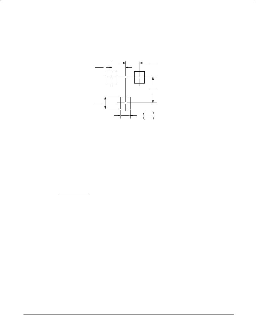
INFORMATION FOR USING THE SOT±23 SURFACE MOUNT PACKAGE
MINIMUM RECOMMENDED FOOTPRINT FOR SURFACE MOUNTED APPLICATIONS
Surface mount board layout is a critical portion of the total design. The footprint for the semiconductor packages must be the correct size to insure proper solder connection
interface between the board and the package. With the correct pad geometry, the packages will self align when subjected to a solder reflow process.
0.037
0.037 0.95
0.95
0.079
2.0
0.035
0.9
0.031 |
inches |
0.8mm
SOT±23
SOT±23 POWER DISSIPATION
The power dissipation of the SOT±23 is a function of the drain pad size. This can vary from the minimum pad size for soldering to a pad size given for maximum power dissipation. Power dissipation for a surface mount device is determined
by TJ(max), the maximum rated junction temperature of the die, RθJA, the thermal resistance from the device junction to
ambient, and the operating temperature, TA. Using the values provided on the data sheet for the SOT±23 package, PD can be calculated as follows:
TJ(max) ± TA
PD = RθJA
The values for the equation are found in the maximum ratings table on the data sheet. Substituting these values into the equation for an ambient temperature TA of 25°C, one can calculate the power dissipation of the device which in this case is 225 milliwatts.
PD = |
150°C ± 25°C |
= 225 milliwatts |
|
556°C/W |
|||
|
|
The 556°C/W for the SOT±23 package assumes the use of the recommended footprint on a glass epoxy printed circuit board to achieve a power dissipation of 225 milliwatts. There are other alternatives to achieving higher power dissipation from the SOT±23 package. Another alternative would be to use a ceramic substrate or an aluminum core board such as Thermal Clad . Using a board material such as Thermal Clad, an aluminum core board, the power dissipation can be doubled using the same footprint.
SOLDERING PRECAUTIONS
The melting temperature of solder is higher than the rated temperature of the device. When the entire device is heated to a high temperature, failure to complete soldering within a short time could result in device failure. Therefore, the following items should always be observed in order to minimize the thermal stress to which the devices are subjected.
•Always preheat the device.
•The delta temperature between the preheat and soldering should be 100°C or less.*
•When preheating and soldering, the temperature of the leads and the case must not exceed the maximum temperature ratings as shown on the data sheet. When
using infrared heating with the reflow soldering method, the difference shall be a maximum of 10°C.
•The soldering temperature and time shall not exceed 260°C for more than 10 seconds.
•When shifting from preheating to soldering, the maximum temperature gradient shall be 5°C or less.
•After soldering has been completed, the device should be allowed to cool naturally for at least three minutes. Gradual cooling should be used as the use of forced cooling will increase the temperature gradient and result in latent failure due to mechanical stress.
•Mechanical stress or shock should not be applied during cooling.
* Soldering a device without preheating can cause excessive thermal shock and stress which can result in damage to the device.
MOTOROLA |
MMBZ15VDLT1 MMBZ27VCLT1 |
64