Материал: tvs2
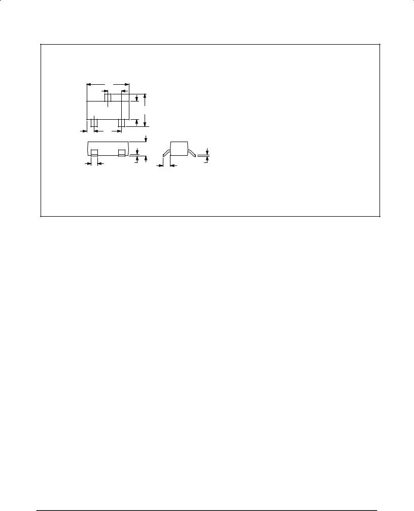
OUTLINE DIMENSIONS
A
L
3
B S
1 |
2 |
V G
|
|
C |
|
D |
H |
K |
J |
|
|
|
CASE 318±08
ISSUE AE
TO±236AB
NOTES:
1.DIMENSIONING AND TOLERANCING PER ANSI Y14.5M, 1982.
2.CONTROLLING DIMENSION: INCH.
3.MAXIUMUM LEAD THICKNESS INCLUDES LEAD FINISH THICKNESS. MINIMUM LEAD THICKNESS IS THE MINIMUM THICKNESS OF BASE MATERIAL.
|
INCHES |
MILLIMETERS |
||
DIM |
MIN |
MAX |
MIN |
MAX |
A |
0.1102 |
0.1197 |
2.80 |
3.04 |
B |
0.0472 |
0.0551 |
1.20 |
1.40 |
C |
0.0350 |
0.0440 |
0.89 |
1.11 |
D |
0.0150 |
0.0200 |
0.37 |
0.50 |
G |
0.0701 |
0.0807 |
1.78 |
2.04 |
H |
0.0005 |
0.0040 |
0.013 |
0.100 |
J |
0.0034 |
0.0070 |
0.085 |
0.177 |
K |
0.0140 |
0.0285 |
0.35 |
0.69 |
L |
0.0350 |
0.0401 |
0.89 |
1.02 |
S |
0.0830 |
0.1039 |
2.10 |
2.64 |
V |
0.0177 |
0.0236 |
0.45 |
0.60 |
STYLE 9:
PIN 1. ANODE
2.ANODE
3.CATHODE
MMBZ15VDLT1 MMBZ27VCLT1 |
MOTOROLA |
|
65

Motorola reserves the right to make changes without further notice to any products herein. Motorola makes no warranty, representation or guarantee regarding the suitability of its products for any particular purpose, nor does Motorola assume any liability arising out of the application or use of any product or circuit, and specifically disclaims any and all liability, including without limitation consequential or incidental damages. ªTypicalº parameters can and do vary in different applications. All operating parameters, including ªTypicalsº must be validated for each customer application by customer's technical experts. Motorola does not convey any license under its patent rights nor the rights of others. Motorola products are not designed, intended, or authorized for use as components in systems intended for surgical implant into the body, or other applications intended to support or sustain life, or for any other application in which the failure of the Motorola product could create a situation where personal injury or death may occur. Should Buyer purchase or use Motorola products for any such unintended or unauthorized application, Buyer shall indemnify and hold Motorola and its officers, employees, subsidiaries, affiliates, and distributors harmless against all claims, costs, damages, and expenses, and reasonable attorney fees arising out of, directly or indirectly, any claim of personal injury or death associated with such unintended or unauthorized use, even if such claim alleges that Motorola was negligent regarding the design or manufacture of the part. Motorola and  are registered trademarks of Motorola, Inc. Motorola, Inc. is an Equal Opportunity/Affirmative Action Employer.
How to reach us: |
|
USA / EUROPE: Motorola Literature Distribution; |
JAPAN: Nippon Motorola Ltd.; Tatsumi±SPD±JLDC, Toshikatsu Otsuki, |
P.O. Box 20912; Phoenix, Arizona 85036. 1±800±441±2447 |
6F Seibu±Butsuryu±Center, 3±14±2 Tatsumi Koto±Ku, Tokyo 135, Japan. 03±3521±8315 |
MFAX: RMFAX0@email.sps.mot.com ± TOUCHTONE (602) 244±6609 HONG KONG: Motorola Semiconductors H.K. Ltd.; 8B Tai Ping Industrial Park, |
|
INTERNET: http://Design±NET.com |
51 Ting Kok Road, Tai Po, N.T., Hong Kong. 852±26629298 |
66 |
◊ |
MMBZ15VDLT1/D |
|
*MMBZ15VDLT1/D* |
|
|
|
MMBZ27VCLT1 |
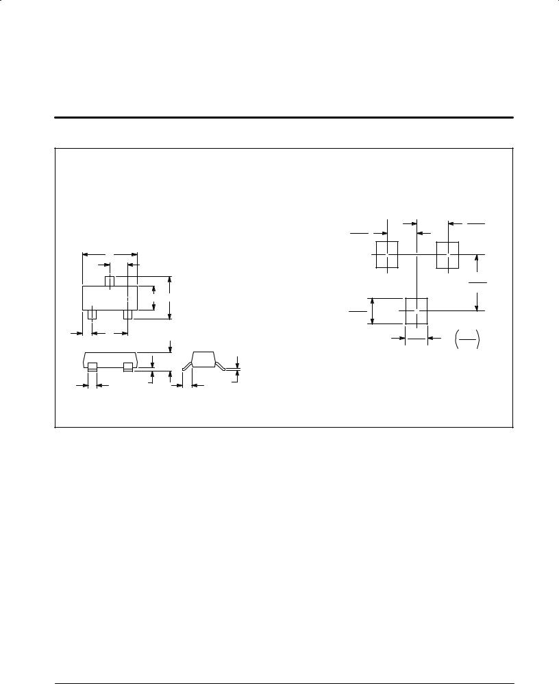
Transient Voltage Suppressors Ð Surface Mounted
40 Watt Peak Power
NOTES:
1.DIMENSIONING AND TOLERANCING PER ANSI Y14.5M, 1982.
2.CONTROLLING DIMENSION: INCH.
3.MAXIMUM LEAD THICKNESS INCLUDES LEAD FINISH THICKNESS. MINIMUM LEAD THICKNESS IS THE MINIMUM THICKNESS OF BASE MATERIAL.
|
A |
|
|
L |
|
|
3 |
S |
|
B |
|
1 |
2 |
|
V |
G |
|
|
INCHES |
MILLIMETERS |
||
DIM |
MIN |
MAX |
MIN |
MAX |
A |
0.1102 |
0.1197 |
2.80 |
3.04 |
B |
0.0472 |
0.0551 |
1.20 |
1.40 |
C |
0.0350 |
0.0440 |
0.89 |
1.11 |
D |
0.0150 |
0.0200 |
0.37 |
0.50 |
G |
0.0701 |
0.0807 |
1.78 |
2.04 |
H |
0.0005 |
0.0040 |
0.013 |
0.100 |
J |
0.0034 |
0.0070 |
0.085 |
0.177 |
K |
0.0180 |
0.0236 |
0.45 |
0.60 |
L |
0.0350 |
0.0401 |
0.89 |
1.02 |
S |
0.0830 |
0.0984 |
2.10 |
2.50 |
V |
0.0177 |
0.0236 |
0.45 |
0.60 |
STYLE 9:
PIN 1. ANODE
2.ANODE
3.CATHODE
|
|
C |
|
D |
H |
K |
J |
CASE 318-07
PLASTIC
0.037
0.037 0.95
0.95
0.079
2.0
0.035
0.9
0.031 |
inches |
0.8mm
SOT-23 Footprint
(Refer to Section 10 for Surface Mount, Thermal Data and Footprint Information.)
MULTIPLE PACKAGE QUANTITY (MPQ)
REQUIREMENTS
Package Option |
Type No. Suffix |
MPQ (Units) |
|
|
|
Tape and Reel |
T1 |
3K |
|
|
|
Tape and Reel |
T3 |
10K |
|
|
|
(Refer to Section 10 for more information on Packaging Specifications.)
Motorola TVS/Zener Device Data |
24 Watt Peak Power Data Sheet |
|
5-67 |
MOTOROLA
SEMICONDUCTOR
TECHNICAL DATA
GENERAL DATA APPLICABLE TO ALL SERIES IN THIS GROUP
Zener Transient Voltage Suppressors
GENERAL
DATA
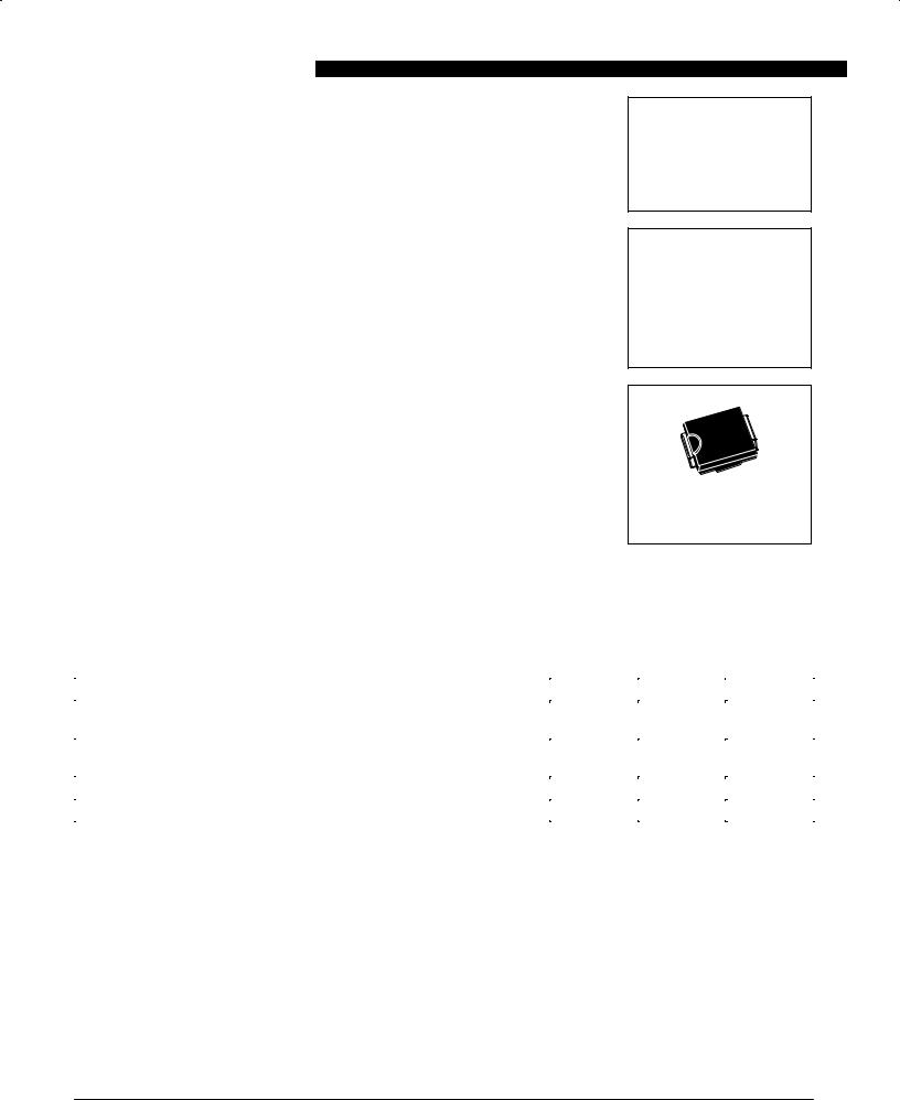
600 WATT
PEAK POWER
The SMB series is designed to protect voltage sensitive components from high voltage, high energy transients. They have excellent clamping capability, high surge capability, low zener impedance and fast response time. The SMB series is supplied in Motorola's exclusive, cost-effective, highly reliable Surmetic package and is ideally suited for use in communication systems, numerical controls, process controls, medical equipment, business machines, power supplies and many other industrial/consumer applications.
Specification Features:
•Standard Zener Breakdown Voltage Range Ð 6.8 to 200 V
•Stand-off Voltage Range Ð 5 to 170 V
•Peak Power Ð 600 Watts @ 1 ms
•Maximum Clamp Voltage @ Peak Pulse Current
•Low Leakage < 5 μA Above 10 V
•UL Recognition
•Response Time Typically < 1 ns
Mechanical Characteristics:
CASE: Void-free, transfer-molded, thermosetting plastic
FINISH: All external surfaces are corrosion resistant and leads are readily solderable POLARITY: Cathode indicated by molded polarity notch. When operated in zener mode,
will be positive with respect to anode
MOUNTING POSITION: Any
LEADS: Modified L-Bend providing more contact area to bond pad
MAXIMUM CASE TEMPERATURE FOR SOLDERING PURPOSES: 260°C for 10 seconds WAFER FAB LOCATION: Phoenix, Arizona
ASSEMBLY/TEST LOCATION: Seremban, Malaysia
MAXIMUM RATINGS
PLASTIC SURFACE MOUNT ZENER OVERVOLTAGE TRANSIENT SUPPRESSORS
6.8±200 VOLTS
600 WATT PEAK POWER
CASE 403A
PLASTIC
|
Rating |
Symbol |
Value |
Unit |
|
|
|
|
|
Peak Power Dissipation (1) |
PPK |
600 |
Watts |
|
@ TL ≤ 25°C |
|
|
|
|
Forward Surge Current (2) |
IFSM |
100 |
Amps |
|
@ TA = 25°C |
|
|
|
|
Thermal Resistance from Junction to Lead (typical) |
RqJL |
25 |
°C/W |
|
Operating and Storage Temperature Range |
TJ, Tstg |
± 65 to +150 |
°C |
|
NOTES: 1. |
Nonrepetitive current pulse per Figure 2 and derated above TA = 25°C per Figure 3. |
|
|
|
2. |
1/2 sine wave (or equivalent square wave), PW = 8.3 ms, duty cycle = 4 pulses per minute maximum. |
|
|
|
REV 1
600 Watt Peak Power Data Sheet |
Motorola TVS/Zener Device Data |
5-68 |
|
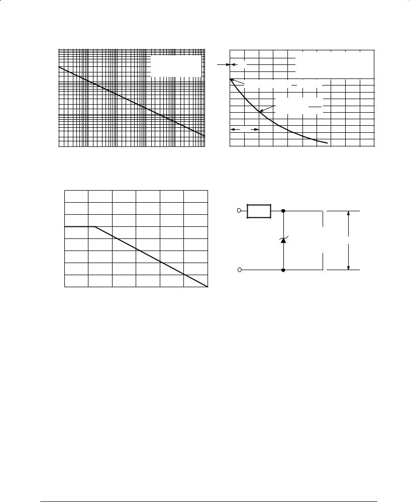
GENERAL DATA Ð 600 WATT PEAK POWER
PP, PEAK POWER (kW)
100 |
|
|
|
|
|
|
|
|
|
PULSE WIDTH (tP) IS DEFINED |
|
|
|
|
|
|
NONREPETITIVE |
|
|
|
|
||
|
|
|
|
|
|
|
tr |
|
AS THAT POINT WHERE THE PEAK |
||
|
|
|
|
|
PULSE WAVEFORM |
|
|
|
|||
|
|
|
|
|
|
|
|
CURRENT DECAYS TO 50% |
|||
|
|
|
|
|
SHOWN IN FIGURE 2 |
|
|
|
|||
|
|
|
|
|
|
|
|
OF IRSM. |
|
||
10 |
|
|
|
|
|
|
100 |
|
|
|
|
|
|
|
|
|
|
PEAK VALUE ± IRSM |
tr ≤ 10 μs |
|
|||
|
|
|
|
|
VALUE(%) |
|
|
||||
|
|
|
|
|
|
|
|
HALF VALUE ± IRSM |
|
||
1 |
|
|
|
|
|
|
50 |
|
|
2 |
|
|
|
|
|
|
|
|
|
|
|
||
|
|
|
|
|
|
|
|
|
|
|
|
|
|
|
|
|
|
|
|
tP |
|
|
|
0.1 |
μs |
1 μs |
10 μs |
100 μs |
|
|
0 |
|
|
|
|
0.1 |
1 ms |
10 ms |
0 |
1 |
2 |
3 |
4 |
||||
tP, PULSE WIDTH |
t, TIME (ms) |
Figure 1. Pulse Rating |
Figure 2. Pulse Waveform |
Curve |
|
|
|
160 |
|
|
|
|
|
|
OF = 25°C |
140 |
|
|
|
|
|
|
|
|
|
|
|
|
|
|
||
% |
A |
120 |
|
|
|
|
|
|
T |
|
|
|
|
|
|
||
IN @ |
|
|
|
|
|
|
||
|
|
|
|
|
|
|
||
PEAK PULSE DERATING |
PEAK POWER OR CURRENT |
100 |
|
|
|
|
|
|
80 |
|
|
|
|
|
|
||
60 |
|
|
|
|
|
|
||
40 |
|
|
|
|
|
|
||
20 |
|
|
|
|
|
|
||
0 |
|
|
|
|
|
|
||
|
|
25 |
50 |
75 |
100 |
125 |
150 |
|
|
|
0 |
||||||
|
|
|
|
TA, AMBIENT TEMPERATURE (°C) |
|
|
||
TYPICAL PROTECTION CIRCUIT
Zin
Vin |
LOAD |
VL |
|
|
|
Figure 3. Pulse Derating Curve
APPLICATION NOTES
RESPONSE TIME
In most applications, the transient suppressor device is placed in parallel with the equipment or component to be protected. In this situation, there is a time delay associated with the capacitance of the device and an overshoot condition associated with the inductance of the device and the inductance of the connection method. The capacitive effect is of minor importance in the parallel protection scheme because it only produces a time delay in the transition from the operating voltage to the clamp voltage as shown in Figure 4.
The inductive effects in the device are due to actual turn-on time (time required for the device to go from zero current to full current) and lead inductance. This inductive effect produces an overshoot in the voltage across the equipment or component being protected as shown in Figure 5. Minimizing this overshoot is very important in the application, since the main purpose for adding a transient suppressor is to clamp voltage spikes. The SMB series have a very good response time, typically < 1 ns and negligible inductance. However, external inductive effects could produce unacceptable overshoot. Proper circuit layout, minimum lead lengths and placing
the suppressor device as close as possible to the equipment or components to be protected will minimize this overshoot.
Some input impedance represented by Zin is essential to prevent overstress of the protection device. This impedance should be as high as possible, without restricting the circuit operation.
DUTY CYCLE DERATING
The data of Figure 1 applies for non-repetitive conditions and at a lead temperature of 25°C. If the duty cycle increases, the peak power must be reduced as indicated by the curves of Figure 6. Average power must be derated as the lead or ambient temperature rises above 25°C. The average power derating curve normally given on data sheets may be normalized and used for this purpose.
At first glance the derating curves of Figure 6 appear to be in error as the 10 ms pulse has a higher derating factor than the 10 μs pulse. However, when the derating factor for a given pulse of Figure 6 is multiplied by the peak power value of Figure 1 for the same pulse, the results follow the expected trend.
Motorola TVS/Zener Device Data |
600 Watt Peak Power Data Sheet |
|
5-69 |